
Data Sheet

1998-2021 Microchip Technology Inc. DS20001203X-page 11
24AA256/24LC256/24FC256
6.0 WRITE OPERATIONS
6.1 Byte Write
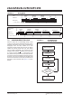
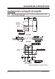
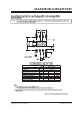
Following the Start condition from the host, the control
code (four bits), the Chip Select (three bits) and the
R/W
bit (which is a logic low) are clocked onto the bus
by the host transmitter. This indicates to the addressed
client receiver that the address high byte will follow
after it has generated an Acknowledge bit during the
ninth clock cycle. Therefore, the next byte transmitted
by the host is the high-order byte of the word address
and will be written into the Address Pointer of the
24XX256. The next byte is the Least Significant
Address Byte. After receiving another Acknowledge
signal from the 24XX256, the host device will transmit
the data word to be written into the addressed memory
location. The 24XX256 acknowledges again and the
host generates a Stop condition. This initiates the
internal write cycle and during this time, the 24XX256
will not generate Acknowledge signals (Figure 6-1). If
an attempt is made to write to the array with the WP pin
held high, the device will acknowledge the command
but no write cycle will occur, no data will be written, and
the device will immediately accept a new command.
After a byte write command, the internal address
counter will point to the address location following the
one that was just written.
6.2 Page Write
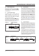
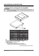
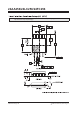
The write control byte, word address and the first data
byte are transmitted to the 24XX256 in much the same
way as in a byte write. The exception is that instead of
generating a Stop condition, the host transmits up to
63 additional bytes, which are temporarily stored in the
on-chip page buffer, and will be written into memory
once the host has transmitted a Stop condition. Upon
receipt of each word, the six lower Address Pointer bits,
which form the byte counter, are internally incremented
by one. If the host should transmit more than 64-bytes
prior to generating the Stop condition, the address
counter will roll over and the previously received data
will be overwritten. As with the byte write operation,
once the Stop condition is received, an internal write
cycle will begin (Figure 6-2). If an attempt is made to
write to the array with the WP pin held high, the device
will acknowledge the command, but no write cycle will
occur, no data will be written and the device will
immediately accept a new command.
6.3 Write Protection
The WP pin allows the user to write-protect the entire
array (0000-7FFF) when the pin is tied to V
CC. If tied to
V
SS the write protection is disabled. The WP pin is
sampled at the Stop bit for every write command
(Figure 1-1). Toggling the WP pin after the Stop bit will
have no effect on the execution of the write cycle.
Note: When doing a write of less than 64 bytes,
the data in the rest of the page are
refreshed along with the data bytes being
written. This will force the entire page to
endure a write cycle, for this reason
endurance is specified per page.
Note: Page write operations are limited to
writing bytes within a single physical page,
regardless of the number of bytes
actually being written. Physical page
boundaries start at addresses that are
integer multiples of the page buffer size
(or page size) and end at addresses that
are integer multiples of page size 1. If a
page write command attempts to write
across a physical page boundary, the
result is that the data wrap around to the
beginning of the current page (overwriting
data previously stored there), instead of
being written to the next page, as might be
expected. It is, therefore, necessary for
the application software to prevent page
write operations that would attempt to
cross a page boundary.