
Data Sheet

24AA256/24LC256/24FC256
DS20001203X-page 10 1998-2021 Microchip Technology Inc.
5.0 DEVICE ADDRESSING
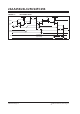
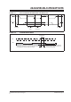
A control byte is the first byte received following the
Start condition from the host device. The control byte
consists of a 4-bit control code. For the 24XX256, this
is set as
1010 binary for read and write operations.
The next three bits of the control byte are the Chip
Select bits (A2, A1, A0). The Chip Select bits allow the
use of up to eight 24XX256 devices on the same bus
and are used to select which device is accessed. The
Chip Select bits in the control byte must correspond to
the logic levels on the corresponding A2, A1 and A0
pins for the device to respond. These bits, in effect, are
the three Most Significant bits of the word address. The
combination of the 4-bit control code and the next three
bits are called the client address.
For the MSOP package, the A0 and A1 pins are not
connected. During device addressing, the A0 and A1
Chip Select bits (Figures 5-1 and 5-2) should be set
to 0. Only two 24XX256 MSOP packages can be
connected to the same bus.
The last bit of the control byte is the Read/Write
(R/W)
bit and it defines the operation to be performed. When
set to 1, a read operation is selected. When set to 0,
a write operation is selected. The next two bytes
received define the address of the first data byte
(Figure 5-2). Because only A14A0 are used, the
upper address bits are a dont care. The upper
address bits are transferred first, followed by the Least
Significant bits.
Following the Start condition, the 24XX256 monitors
the SDA bus checking the device type identifier being
transmitted. Upon receiving a
1010 code and
appropriate device select bits, the client device outputs
an Acknowledge signal on the SDA line. Depending on
the state of the R/W
bit, the 24XX256 will select a read
or write operation.
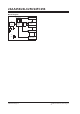
FIGURE 5-1: CONTROL BYTE
FORMAT
5.1 Contiguous Addressing Across
Multiple Devices
The Chip Select bits A2, A1 and A0 can be used to
expand the contiguous address space for up to 2-Mbit
by adding up to eight 24XX256 devices on the same
bus. In this case, software can use A0 of the control
byte as address bit A15; A1 as address bit A16; and A2
as address bit A17. It is not possible to sequentially
read across device boundaries.
For the MSOP package, up to two 24XX256 devices
can be added for up to 512-Kbit of address space. In
this case, software can use A2 of the control byte as
address bit A17. Bits A0 (A15) and A1 (A16) of the
control byte must always be set to a logic 0 for the
MSOP.
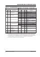
FIGURE 5-2: ADDRESS SEQUENCE BIT ASSIGNMENTS
10
1
0 A2 A1 A0SACKR/W
Control Code
Chip Select
Bits
Client Address
Acknowledge Bit
Start Bit
Read/Write
Bit
1010
A
2
A
1
A
0
R/W x
A
11
A
10
A
9
A
7
A
0
A
8
A
12
Control Byte Address High Byte Address Low Byte
Control
Code
Chip
Select
Bits
x = dont care bit
A
13
A
14