
Datasheet
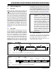

24AA02E48/24AA025E48/24AA02E64/24AA025E64
DS20002124E-page 6 2008-2013 Microchip Technology Inc.
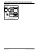
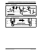
2.0 PIN DESCRIPTIONS
The descriptions of the pins are listed in Tab le 2- 1.
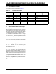
TABLE 2-1: PIN FUNCTION TABLE
2.1 Serial Address/Data Input/Output
(SDA)
SDA is a bidirectional pin used to transfer addresses
and data into and out of the device. Since it is an open-
drain terminal, the SDA bus requires a pull-up resistor
to V
CC (typical 10 k for 100 kHz, 2 k for 400 kHz).
For normal data transfer, SDA is allowed to change
only during SCL low. Changes during SCL high are
reserved for indicating Start and Stop conditions.
2.2 Serial Clock (SCL)
The SCL input is used to synchronize the data transfer
to and from the device.
2.3 A0, A1, A2 Chip Address Inputs
The A0, A1 and A2 pins are not used by the
24AA02E48/24AA02E64. They may be left floating or
tied to either VSS or VCC.
For the 24AA025E48/24AA025E64, the levels on the
A0, A1 and A2 inputs are compared with the
corresponding bits in the slave address. The chip is
selected if the compare is true. For the 6-lead SOT-23
package, pin A2 is not connected and its corresponding
bit in the slave address should always be set to ‘0’.
Up to eight 24AA025E48/24AA025E64 devices (four
for the SOT-23 package) may be connected to the
same bus by using different Chip Select bit combina-
tions. These inputs must be connected to either V
SS or
V
CC.
Name SOIC 5-Pin SOT-23 6-Pin SOT-23 Description
A0 1 — 5 Chip Address Input
(1)
A1 2 — 4 Chip Address Input
(1)
A2 3 — — Chip Address Input
(1)
VSS 422Ground
SDA 5 3 3 Serial Address/Data I/O
SCL 6 1 1 Serial Clock
NC 7 5 — Not Connected
V
CC 8 4 6 +1.7V to 5.5V Power Supply
Note 1: Chip address inputs A0, A1 and A2 are not connected on the 24AA02E48/24AA02E64.