
Datasheet


2008-2013 Microchip Technology Inc. DS20002124E-page 11
24AA02E48/24AA025E48/24AA02E64/24AA025E64
8.0 READ OPERATION
Read operations are initiated in the same way as write
operations, with the exception that the R/W
bit of the
slave address is set to ‘
1’. There are three basic types
of read operations: current address read, random read
and sequential read.
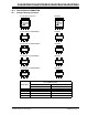
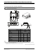
8.1 Current Address Read
The 24AA02XEXX contains an address counter that
maintains the address of the last word accessed, inter-
nally incremented by ‘
1’. Therefore, if the previous
access (either a read or write operation) was to address
n, the next current address read operation would
access data from address
n + 1. Upon receipt of the
slave address with R/W
bit set to ‘1’, the 24AA02XEXX
issues an acknowledge and transmits the 8-bit data
word. The master will not acknowledge the transfer, but
does generate a Stop condition, and the 24AA02XEXX
discontinues transmission (Figure 8-1).
8.2 Random Read
Random read operations allow the master to access
any memory location in a random manner. To perform
this type of read operation, the word address must first
be set. This is accomplished by sending the word
address to the 24AA02XEXX as part of a write
operation. Once the word address is sent, the master
generates a Start condition following the acknowledge.
This terminates the write operation, but not before the
internal Address Pointer is set. The master then issues
the control byte again, but with the R/W
bit set to a ‘1’.
The 24AA02XEXX will then issue an acknowledge and
transmit the 8-bit data word. The master will not
acknowledge the transfer, but does generate a Stop
condition, and the 24AA02XEXX will discontinue
transmission (Figure 8-2).
8.3 Sequential Read
Sequential reads are initiated in the same way as a
random read, except that once the 24AA02XEXX
transmits the first data byte, the master issues an
acknowledge as opposed to a Stop condition in a ran-
dom read. This directs the 24AA02XEXX to transmit the
next sequentially-addressed 8-bit word (Figure 8-3).
To provide sequential reads, the 24AA02XEXX
contains an internal Address Pointer that is
incremented by one upon completion of each opera-
tion. This Address Pointer allows the entire memory
contents to be serially read during one operation.
8.4 Noise Protection
The 24AA02XEXX employs a VCC threshold detector
circuit which disables the internal erase/write logic if the
V
CC is below 1.5V at nominal conditions.
The SCL and SDA inputs have Schmitt Trigger and
filter circuits which suppress noise spikes to assure
proper device operation, even on a noisy bus.
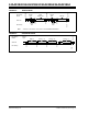
FIGURE 8-1: CURRENT ADDRESS READ
SP
Bus Activity
Master
SDA Line
Bus Activity
S
T
O
P
Control
Byte
Data (n)
A
C
K
N
o
A
C
K
S
T
A
R
T
1
01
0
A2* A1*
A0*
1
Chip
Select
Bits
Note: * Bits A0, A1 and A2 are “don’t cares” for the 24AA02E48/24AA02E64.