
Single-Line Laser Scan Engine Integration Guide


Table Of Contents
- IS4813, IS4815, IS4823 and IS4825
- Copyright/Trademarks
- Table Of Contents
- Introduction
- Assembly
- Mounting Specifications
- IS4813 and IS4815 Scan Engine Dimensions
- IS4823 and IS4825 Bracketed (-1 and -2) Dimensions
- IS4823 and IS4825 (-0) Decode Printed Circuit Board Dimensions
- Exit Beam Specifications
- Enclosure Specifications
- Electrostatic Discharge (ESD) Cautions
- Grounding
- Power Supply
- Power Sequencing
- Flex Cables
- Thermal Considerations
- Printed Circuit Board (PCB) Component Clearance
- Magnetic Sensitivity
- Airborne Contaminants and Foreign Materials
- Beam Clearance
- Output Window Properties
- Output Window Coatings
- Output Window Angle
- Minimum Allowable Window Position RequiredTo Avoid Detrimental Internal Reflective Beam Interference at Positive Exit Beam Angle Tolerance
- Minimum Allowable Window Position Required To Avoid Detrimental Internal Reflective Beam Interference at Negative Exit Beam Angle Tolerance
- Scan Engine Field Of View And Depth Of Field
- Descriptions Of IS4823 AND IS4825 Operating Modes
- Serial Configuration Mode
- General Design Specifications
- Detailed Electrical Specifications
- Scan Engine Terminations
- Decode Printed Circuit Board Terminations
- Flex Cable Specifications And Installation Guidelines
- Timing Diagrams
- Bar Code Element Time Calculation
- Regulatory Compliance
- Limited Warranty
- Patents
- Index
- Contact Information
- MANUAL DATE CODE
23
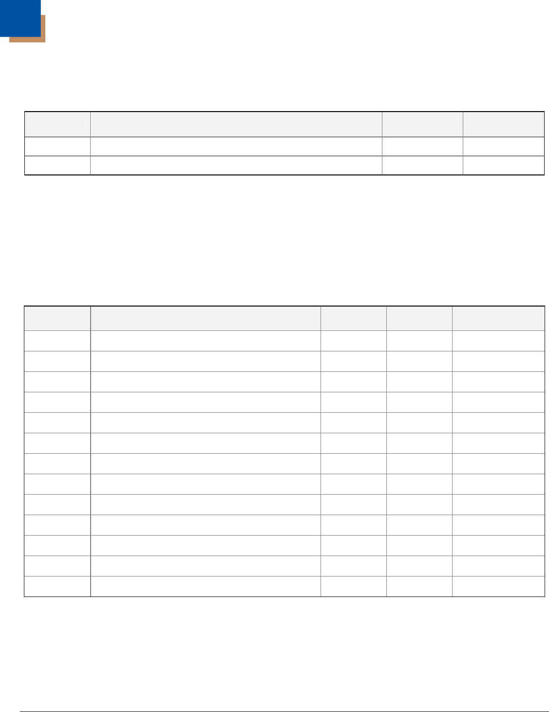
Detailed Electrical Specifications
Absolute Maximum Ratings
Signal Signal Description Minimum Maximum
Vinput
†
Voltage Applied to Any input pin (except D+ and D-) * -0.3V Vin
Voutput Voltage Applied to Any output pin ** -0.3V Vin + 0.3V
* For USB version, Voltages on D+ and D- signal must conform to USB Specification
** Voutput must be less than 5.5V for all pins
†
If the Vinput signal is greater than VIN, current will flow from the input to the VIN pin through the
pull up resistors on the engine. In Suspend Mode, this may cause current to flow into the USB power.
This is not recommended.
IS4823 DC Operating Voltages
Signal Signal Description Minimum Maximum Condition
VIN Operating Voltage 3.0V 3.6V
VIH(1) Input High (RX, CTS) 2.5V
VIL(1) Input Low (RX, CTS) 0.8V
VIH(2) Input High (TTL_INV, nWake) 0.8 x Vin
VIL(2) Input Low (TTL_INV, nWake) 0.8V
VIH(3) Input High (EXT. Trigger) 0.8 x Vin
VIL(3) Input Low (EXT. Trigger) 0.8V
VOH(1) Output High Voltage (TX,RTS) 0.8 x Vin Isource = 16 mA
VOL(1) Output Low Voltage (TX,RTS) 0.14 x Vin Isink = 16 mA
VOH(2) Output High Voltage (nBeeper, nGoodRead)
***
3.6V
VOL(2) Output Low Voltage (nBeeper, nGoodRead) 1.6V Isink = 25 mA
VOH(3) Output High Voltage (Power down)
***
3.6V
VOL(3) Output Low Voltage (Power down) 0.2V Isink = 8 mA
***
PWRDWN, nGoodRead, and nBeeper are open drain outputs w/ 100K pull-ups to VIN. Actual VOH will be determined
by the parallel resistance of the 100K pull up and any external impedance.