
Datasheet

Detailed Description
The MAX3180–MAX3183 are EIA/TIA-232 and V.28/
V.24 communications receivers that convert RS-232
signals to CMOS logic levels. The devices operate on a
supply voltage of +3V to +5.5V and have a 1.5Mbps
data rate capability. They achieve a 0.5µA typical sup-
ply current. The MAX3180/MAX3182 have a receiver
enable control (EN), while the MAX3181/MAX3183 con-
tain a signal invalid output (INVALID). The MAX3180/
MAX3181 invert the ROUT signal relative to RIN. The
MAX3182/MAX3183 are not inverted. The devices
come in SOT23-5 packages.
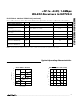
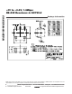
Signal Invalid Detector
If no valid signal levels appear on RIN for 30µs (typ),
INVALID goes low. This event typically occurs if the RS-
232 cable is disconnected or if the connected peripher-
al transmitter is turned off. INVALID goes high when a
valid level is applied to the RS-232 receiver input.
Figure 2 shows the input levels and timing diagram for
INVALID operation.
Enable Input
The MAX3180/MAX3182 feature an enable input. Drive
EN high to force ROUT into a high-impedance state. In
this state, the devices ignore incoming RS-232 signals.
Drive EN low for normal operation.
Power-Supply Decoupling
In most circumstances, a 0.1µF V
CC
bypass capacitor
is adequate for power-supply decoupling. Connect the
bypass capacitor as close to the IC as possible.
MAX3180–MAX3183
+3V to +5.5V, 1.5Mbps
RS-232 Receivers in SOT23-5
_______________________________________________________________________________________ 5
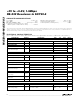
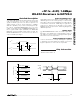
50% 50%
50%
0
RIN
5V
ROUT
50%
t
PLH
t
PHL
V
OL
V
OH
Figure 1. Receiver Propagation-Delay Timing
VALID SIGNALS (INVALID = 1)
INVALID SIGNALS (INVALID = 0)
VALID SIGNALS (INVALID = 1)
RECEIVER INPUT LEVELS
-2.7V
-0.3V
+2.7V
+0.3V
0
INDETERMINATE
INDETERMINATE
0
V
CC
t
INVL
INVALID
REGION
RECEIVER
INPUT
VOLTAGE
(V)
INVALID
OUTPUT
(V)
t
INVH
Figure 2. Input Levels and INVALID Timing
Chip Information
TRANSISTOR COUNT: 41