
Specifications


Table Of Contents
- Table of Contents
- 1. Board Floorplan
- 2. PCB Errata
- 3. File Locations
- 4. Basic Operation
- 5. Jumpers and Connectors
- 6. Line-Side Connections
- 7. System Connectors
- 8. Microcontroller
- 9. Power-Supply Connectors
- 10. Connecting to a Computer
- 11. Installing and Running the Software
- 12. Address Map
- 13. Additional Information/Resources
- 14. Component List
- 15. Schematics
_________________________________________________________________________________________________
DS33M33DK
Rev: 102108 14 of 48
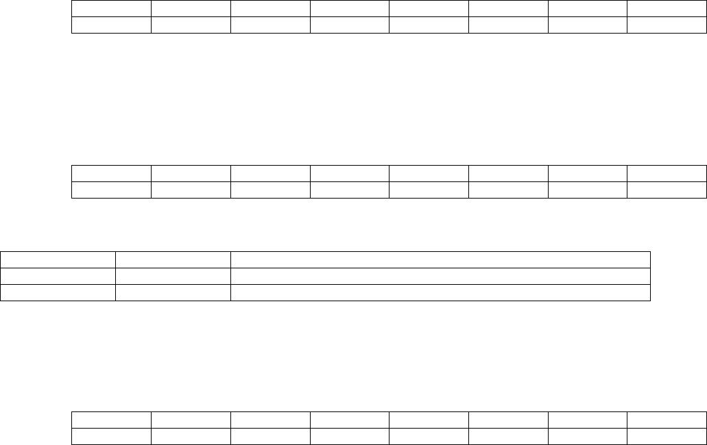
Register Name: DTOH_STAT
Register Description: DTOH Status
Register Offset: 0x0005
Bit # 7 6 5 4 3 2 1 0
Name STAT7 STAT6 STAT5 STAT4 STAT3 STAT2 STAT1 STAT0
Default 0 0 0 0 0 0 0 0
Read value of 1 of 81 bytes selected by DTOH_SEL.
Register Name: DTOH_SEL
Register Description: DTOH Configuration
Register Offset: 0x0006
Bit # 7 6 5 4 3 2 1 0
Name SEL7 SEL6 SEL5 SEL4 SEL3 SEL2 SEL1 SEL0
Default 0 0 0 0 0 0 0 0
Byte select for overhead transport byte, the overhead byte specified by DTOH_CFG is written to DTOH_STAT.
Examples:
DTOH_SEL DTOH_STAT RESULT
0 First byte The first byte of the transport overhead is written to DTOH_STAT.
0x80 Last byte The last byte of the transport overhead is written to DTOH_STAT.
Register Name: GPIOrd_STAT
Register Description: GPIO Read Values
Register Offset: 0x0007
Bit # 7 6 5 4 3 2 1 0
Name — GPIOA3 GPIOA2 GPIOA1 — GPIOB3 GPIOB2 GPIOB1
Default 0 0 0 0 0 0 0 0
Bit 6: DS33M33 GPIOA3 Pin Value
Reflects the value of DS33M33 GPIOA3 pin.
Bit 5: DS33M33 GPIOA3 Pin Value
Reflects the value of DS33M33 GPIOA2 pin.
Bit 4: DS33M33 GPIOA3 Pin Value
Reflects the value of DS33M33 GPIOA1 pin.
Bit 2: DS33M33 GPIOA3 Pin Value
Reflects the value of DS33M33 GPIOB3 pin.
Bit 1: DS33M33 GPIOA3 Pin Value
Reflects the value of DS33M33 GPIOB2 pin.
Bit 0: DS33M33 GPIOA3 Pin Value
Reflects the value of DS33M33 GPIOB1 pin.