Rev: 102108 DS33M33 Demo Kit General Description The DS33M33 demo kit (DK) is an easy-to-use evaluation board for the DS33M33 and the DS33M33 Ethernet-over-SONET/SDH devices. The demo kit contains an option for either T3 or E3. The T3E3 links are complete with line interface, transformers, and network connections. Maxim’s ChipView software is provided with the demo kit, giving point-and-click access to configuration and status registers from a Windows®-based_PC.
_________________________________________________________________________________________________ DS33M33DK Table of Contents 1. BOARD FLOORPLAN ..................................................................................................................... 3 2. PC BOARD ERRATA....................................................................................................................... 3 3. FILE LOCATIONS ...................................................................................
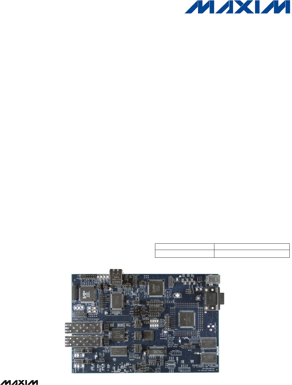
_________________________________________________________________________________________________ DS33M33DK 1. Board Floorplan Figure 1-1.
_________________________________________________________________________________________________ DS33M33DK 3. File Locations This demo kit relies upon several supporting files, which are provided on the CD and are available as a zip file from the Maxim website www.maxim-ic.com/DS33M33DK. All locations are given relative to the directory in the CD/zip file called “DS33M33_def_ini_”. Table 3-1 shows the DS33M33, DS3154, and FPGA register definition files and configuration files. Table 3-1.
_________________________________________________________________________________________________ DS33M33DK 4. Basic Operation Note: In the following sections, software-related items are identified by bolding. Text in bold refers to items directly from the EV kit software. Text in bold and underlined refers to items from the Windows operating system. 4.1 • • • Powering Up the Demo Kit Connect PCB power jack to the wall adapter. Connect RS232 serial cable, or USB cable between the host PC and demo kit.
_________________________________________________________________________________________________ DS33M33DK network traffic is sent out the default adapter, which usually is the adapter that has recently had connection to a live network. 5. Jumpers and Connectors Jumpers and connectors are listed in Table 5-1. They are listed in order of appearance on the PCB from left to right, top to bottom (as viewed with SONET connectors port on the left side of the board). Table 5-1.
_________________________________________________________________________________________________ DS33M33DK SILKSCREEN REFERENCE FUNCTION BASIC SETTING SCHEMATIC PAGE DESCRIPTION P2+3 PHY clock to mac output is disabled, P1+2 PHY clock to mac output is enabled. Mac clock only needs to be enabled in Gigabit mode. Flashes for PHY Tx-Rx activity. LED to indicate link speed–1000, 100, or 10Mbps. Only one of the three LEDs should be lit. See JP05 + JP02 description for setting in GMII vs. MII mode.
_________________________________________________________________________________________________ DS33M33DK SILKSCREEN REFERENCE J09 J10 J03 J04 DS02 DS03 DS08 DS09 DS05 DS04 J06 J07 FUNCTION BASIC SETTING SCHEMATIC PAGE DESCRIPTION Test points to view analog +differential SerDes signals. To loopback DS33M33 Tx→Rx remove the SFP and jumper P3+5 and P2+6. SerDes analog test points — 3, 4 SFP test points Jumper P9+10 3 Test points for SFP module.
_________________________________________________________________________________________________ DS33M33DK 6. Line-Side Connections The DS33M33DK has two optical ports: one Ethernet port and three T3E3 ports. 7. System Connectors System-side signals can be accessed from test point headers. The headers are clearly labeled with signal information. 8. Microcontroller The microcontroller has factory-installed firmware in on-chip nonvolatile memory.
_________________________________________________________________________________________________ DS33M33DK 11. Installing and Running the Software ChipView is a general-purpose program that supports a number of Maxim demo kits. To install the ChipView software, run Chipview.msi from the disk included in the DS33M33DK box or from the zip file downloadable on our website at www.maxim-ic.com/DS33M33DK. After installation, run the ChipView program with the DS33M33DK board powered up and connected to the PC.
_________________________________________________________________________________________________ DS33M33DK 12. Address Map Address space begins at 0x81000000. All offsets given in the following tables are relative to 0x81000000. Registers in the FPGA can be easily modified using the ChipView host-based user interface software along with the definition file named Overhead_FPGA.def. Table 12-1.
_________________________________________________________________________________________________ DS33M33DK 12.2 Control and Status Registers Register Name: ATOH_CFG Register Description: ATOH Configuration Register Offset: 0x0001 Bit # Name Default 7 6 5 4 3 2 1 0 0 0 0 0 0 0 0 0 This register sets the overhead transport data byte value, which is positioned by the following register, ATOHEN_CFG.
_________________________________________________________________________________________________ DS33M33DK Register Name: GPIOAwr Register Description: GPIO A Output Enable + Write Value Register Offset: 0x0003 Bit # Name Default 7 6 — — 0 0 5 GPIOa3 Output En 0 4 GPIOa3 Value 0 3 GPIOa2 Output En 0 2 GPIOa2 Value 0 1 GPIOa1 Output En 0 0 GPIOa1 Value 0 3 GPIOb2 Output En 0 2 GPIOb2 Value 0 1 GPIOb1 Output En 0 0 GPIOb1 Value 0 Bits 5 and 4: DS33M33 GPIOA_3 Three-State and Level 0x = FPGA
_________________________________________________________________________________________________ DS33M33DK Register Name: DTOH_STAT Register Description: DTOH Status Register Offset: 0x0005 Bit # Name Default 7 STAT7 0 6 STAT6 0 5 STAT5 0 4 STAT4 0 3 STAT3 0 2 STAT2 0 1 STAT1 0 0 STAT0 0 4 SEL4 0 3 SEL3 0 2 SEL2 0 1 SEL1 0 0 SEL0 0 Read value of 1 of 81 bytes selected by DTOH_SEL.
_________________________________________________________________________________________________ DS33M33DK Register Name: RDOH_STAT Register Description: RDOH Status Register Offset: 0x0008 Bit # Name Default 7 — 0 6 — 0 5 — 0 4 — 0 3 — 0 2 — 0 1 — 0 0 — 0 1 B1 0 0 B0 0 Read value from the member and byte selected by RDOH_SEL[7:4] and RDOH_SEL[3:0] Register Name: RDOH_SEL Register Description: RDOH Select Register Offset: 0x000A Bit # Name Default 7 IF3 0 6 IF2 0 5 IF1 0 4 IF0 0 3 B3 0 2
_________________________________________________________________________________________________ DS33M33DK 13. Additional Information/Resources 13.1 DS33M33 Information For more information about the DS33M33, refer to the DS33M33 data sheet at www.maxim-ic.com/DS33M33. 13.2 DS33M33DK Information For more information about the DS33M33DK, refer to the DS33M33DK Quick View page at www.maxim-ic.com/DS33M33DK. 13.3 Technical Support For additional technical support, submit your questions at www.maxim-ic.
_________________________________________________________________________________________________ DS33M33DK 14. Component List DESIGNATION QTY DESCRIPTION SUPPLIER PART C08, CB34, CB36, CB37, CB38, CB39, CB40, CB41, CB42, CB58, CB64, CB66, CB67, CB68, CB72, CB79, CB92, CB101, CB104, CB112, CB170 21 L_0603 CERAM .01uF 50V 10% X7R AVX 06035C103KAT See next row (begins with C02) 61 L_0603 CERAM .
_________________________________________________________________________________________________ DS33M33DK CB50, CB56, CB57, CB61, CB71, CB80, CB81, CB87, CB99, CB105, CB108, CB149, CB151, CB152, CB155, CB161, CB166, CB172, CB179, CB180 See next row (begins with C17) 21 1206 CERAM 10uF 10V 20% Panasonic ECJ-3YB1A106M C17, C19, C20, C21, C22, C24, CB188 , CB01, CB02, CB08, CB13, CB35, CB48, CB51, CB52, CB59, CB111, CB124, CB125, CB130, CB169 CB164, CB184 CB178 2 1 L_1206 CERAM 1uF 16V 10% 1206 CERAM
_________________________________________________________________________________________________ DS33M33DK HEADER, 14 PIN, DUAL ROW, VERT Samtec HDR-TSW-107-14T-D CONNECTOR, SINGLE LEVEL, GIGABIT RJ-45, 10 PIN IC, FPGA, 1.2V, 20X20 TQFP, 144 PIN IC, FPGA, 1.
_________________________________________________________________________________________________ DS33M33DK JB09 1 JB03 1 U02, U03 2 CONN 2.1MM/5.5MM PWRJACK RT ANGLE PCB, closed frame, high current 24VDC@5A also requires 5V ACDC adapter INPUT 100-240VAC 50-60HZ 0.6A OUTPUT DC 5V 2.6A. PN DMS050260-P5P-SZ. MODEL 3Z161WP05 PLUG, SMD, 50 PIN, 2 ROW VERTICAL SFP host / receptacle HB01, HB02, HB03, HB04, HB05 5 Rubber bumper 0.
_________________________________________________________________________________________________ DS33M33DK 15. Schematics The DS33M33DK schematics are featured in the following pages. The schematic contains five hierarchal blocks: Microcontroller, DS3154, Ethernet PHY, Ethernet Test Points, and Overhead CPLD. All signals inside a hierarchy block are local, with exception for VCC and ground.
8D6 A B C D 8B2 CS_X2 CS_X3 TE3_L_CS CPLD_CS 6B4 16B3v RESET_LAN RESET_SYS ADDR<13..0> 8 6A5 25MHZOSC_TO_PROC 17C6v 9B1 1B5 10B4 13B6v 1A2 8B5 10B5 9C1 17C4v 17A5v 11B3 1B1 8B3 WR_RW 17A5v DATA<7..0> PROC_OSCIN RESET_OUT RESET_IN 7 A_DUT_<13..0> D_DUT<7..0> WR_RW HIERARCHY SPI_SCK SPI_CS SPI_MOSI 6 BLOCK NAME: MISC_IO<12..1> EN_SOURCE_TIME ENABLE_DRV ENABLE_CLBK SPI_MISO BLOCK MICROPROCESSOR _motprocrescard_dn P.1,13-18 P.2,10,23-24 P.2,9,20-22 P.3-4 P.
A B C : 8 8 @\_RC_LIB\.
A B C : 8 THIS SUBCIRCUIT IS NOT FOR PRODUCTION .
A B C : 8 THIS SUBCIRCUIT IS NOT FOR PRODUCTION .
A B C : 8 8 @\_RC_LIB\.\_RC_TOP_DN_\(SCH_1):PAGE5 7 7 6C3 6 TXD[3] 7 R4 1 2 3 4 3 2 1 0 _rc_top_dn_. ETH_TXD<7..
A B C D GND 1 OSC GND 1 OUT OUT VCC 5 8 8 4 1 25.000MHZ_3.3V_SOCKET 19.44MHZ_3.3V_SOCKET 4 1 OSC YB01 I24 VCC 77.76MHZ_3.3V_SOCKET 4 1 1UH YB02 L01 25B1v 5 8 5 8 4 3 2 1 6B1 7 6C3 30 I22 5 3 1 J19 6 4 2 1D3 10B7 6 4 2 4 3 2 1 6 30 _rc_top_dn_.
A 8 DDR_RAS DDR_WE DDR_CKE DDR_CKINV DDR_CK DDR_CS DDR_LDM DDR_UDM 7C3 7C3 7C3 7C3 7C3 7C3 7C3 7C3 V2_5 DDR_CAS 7C3 12 11 10 9 8 7 6 5 4 3 2 DDR_BA1 4.7UF 7C3 CB74 DDR_BA0 .1UF B CB110 1 A8 B8 D10 A10 A9 B9 C9 C10 D9 D11 C11 B10 A11 C12 B11 A12 B12 A13 B13 A14 C14 D13 C13 .1UF 7B3 4.
A B 5 6 1K 8 4 3 1 2 8C1 7 1B8 8 1D3 M3X_MT2 1B5 1C5 1C5 1C5 1C5 4 5 6 7 RPB29 8 10K 1B1 8D6 5 6 8B3 1A8 8C6 8B3 1A8 1A8 V3_3 8B3 M3X_TEST_EN 6 8 M3X_JTDI M3X_JTDO V3_3 10 4 2 GND 7 5 3 1 J16 7 9 7 5 3 1 FOR INT 5 6 CONN_10P VCC TDO TDI TCK TMS PULLUP M3X_JTCLK M3X_JTMS INSTANTIATE 4 330 7 2 3 RPB53 8 1 10B5 10B5 10B5 8D6 FPGA 1C5 V3_3 6 BLOCK NAME: M3X_JTRST_N IN DS28 V3_3 1B1 1B1 8D4 1B1 8D3 6 DATA<7..
A B C D M33_RCLK1 F3 9C1 9C1 9C1 9C1 9D1 H3 8 M33_RPOS3 M33_RCLK3 M33_RNEG3 RNEG/RLCV K4 RPOS/RDAT RLCLK J3 PORT M33_GPIOA2 M33_GPIOB2 H5 J6 GPIOA GPIOB 7 PORT M33_GPIOB3 K3 GPIOB BLOCK NAME: 6 M33_GPIOA3 L4 GPIOA M33_TPOS3 M33_TNEG3 TPOS/TDAT J5 K5 TNEG TLCLK M33_TCLK3 M33_TPOS2 G5 TPOS/TDAT J4 M33_TNEG2 H6 TNEG TLCLK M33_TCLK2 M33_GPIOB1 F2 GPIOB G3 M33_GPIOA1 G2 GPIOA 10C4 10C4 10C4 10C4 10C4 10C4 _rc_top_dn_.
A 8 2B7 2B7 23A5v 23A4v CPLD_RDOH CPLD_RDOHSOF CPLD_RDOHVLD CPLD_TAOHSOF CPLD_TAOHVLD CPLD_RDOH CPLD_RDOHSOF CPLD_RDOHVLD CPLD_TAOHSOF CPLD_TAOHVLD 23D7v 6A7 9B2 CPLD_OHCLK CPLD_OHCLK 23D7v CPLD_OH1 CPLD_OH1 1D2 1D2 1D3 CP_DUT_CLKC M3X_CLKC 6 BLOCK NAME: CP_DUT_CLKB M3X_CLKB 7 CP_DUT_CLKA M3X_CLKA CP_DUT_CLADCLK CPLD_DTOHSOF CPLD_DTOHSOF M3X_CLADCLK CPLD_DTOHCLK CPLD_DTOHCLK 9B2 2C7 23A6v CPLD_DTOH CPLD_DTOH 23D7v 2C7 23A6v CPLD_ATOHSOF CPLD_ATOHSOF 6C6 2
A B V5_0 8 4.7UF CB156.1UF CB1634.7UF IN4 RST SHDN 5 6 7 IN2 IN3 3 4 RST SHDN 6 7 IN4 IN1 7 1.8V 10 17 GND 11 15 14 13 GND SET OUT4 OUT3 OUT2 OUT1 12 17 GND MAX1793_U 2 5 2.5V 10 11 15 14 13 GND SET OUT4 OUT3 OUT2 UB09 IN3 C13 IN2 CB144.1UF .01UF 3 V1_8 CB139 BLOCK NAME: 6 V2_5 1 .1UF _rc_top_dn_. 330 CB52 10UF CB109 RB28 4.7UF CB87 4.7UF 330 V2_5 4 CB140 .1UF .1UF CB187 .
A B 8 GND_TP03 IN3 IN4 RST SHDN 4 5 6 7 10 17 GND 7 GND_TPB01 1 6 BLOCK NAME: GND_TP02 GND_TP01 GND_TP11 11 15 14 13 GND SET OUT4 OUT3 OUT2 OUT1 1% REGULATOR SHDN IN4 5 RST IN3 4 7 IN2 3 6 IN1 GND_TP04 GND_TPB02 17 GND 12 10 11 15 14 13 GND SET OUT4 OUT3 OUT2 12 68UF 2 OUT1 MAX1793_U UB10 IN2 3.3V IN1 3 CB159 C19 10UF 2 R04 0.0 C21 10UF _rc_top_dn_. R02 0.0 UB11 V3_3 4.7UF 5 4.7UF CB13 CB154 CB153 PARENT BLOCK: 470UF 3.
A B C 54 55 56 57 58 61 ICOC21 ICOC20 ICOC13 ICOC12 ICOC11 ICOC10 70 PROCSER_IN 8 69 68 SCI2_IN PROCSER_OUT 66 SCI2_OUT TEST 63 53 ICOC22 GND 52 ICOC23 RXD1 TXD1 RXD2 TXD2 TEST ICOC10 ICOC11 ICOC12 ICOC13 ICOC20 ICOC21 ICOC22 ICOC23 U09 INT6* D 8 7 MMC2107 CONTROL INT7* 89 7 15D5 @\_RC_LIB\.\_RC_TOP_DN_\(SCH_1):PAGE2_I10@\_RC_LIB\.
A B 16D4 14A5 8 13A1 14A2 13A2 ENABLE 13D3 4 25 13 12 PA<19..
A B C D 13A7 8 15B8 PRT1_IN PRT1_OUT 8 PRT1_IN 15A8 15B8 7 PRT1_OUT 15A8 5 4 3 2 1 2 330 1 RB26 E D C B A J34 J H G F FORCEOFF* VCC R1IN T1OUT R1OUT FORCEON T1IN T2IN INVALID* R2OUT 9 8 7 6 7 4 6 BLOCK NAME: 5 6 7 10K 1 V3_3 18C2 JP26 UART_DIGOUT 15B8 15B2 15B8 15B2 5 RESET_IN 15B2 CB177 4.
A B C 4 5 6 8 GND 8MBIT CS* SCK SO SI I37 7 AT26DF081_U 4 HOLD* WP* 3 7 VCC 8 THIS MEMORY IS FOR SERIAL BOOT (IF USED) SPI_SCK 13B5 16C5 16C6 1A6^ 10K 7 2 3 I40 RPB54 8 1 V3_3 UB06 3.3V 7 1 6 2 5 16B5 PROC_CS 6 16B8 1A6^ 1B6^ 1A6^ _motprocrescard_dn.
8 13A7 1A8^ 7 1B8^ PA<19..0> CS_X3 CS_X2 PROC_OSCIN 14C1 14C1 13A7 14D2 14D2 1B8^ PR29A 80 INT4 (D0) (D6) BANK 2 SPI_MOSI 7 5 6 5 LATTICE D_DUT<7..0> _motprocrescard_dn. 14C1 BANK 3/8 RD_DS CS_X1 0 1 2 3 4 5 6 7 8 9 113 114 115 116 118 119 121 122 123 125 126 129 130 PT24B PT24A PT22B PT22A PT20B PT20A PT18B PT18A PT16A PT14B PT14A PT12B(PCLKC1_0) PT12A(PCLKT1_0) 12 13 0 2 1 3 PARENT BLOCK: \_rc_top_dn_\ 4 A_DUT_<13..
A 8 18B2 3 2 6 1 MEM_SO MEM_SCK MEM_CS 18B2 18B2 18B5 18B2 VCC TDO TDI TCK 2 3 1 CS* SCK SO SI UB04 I15 2.
A B C D IO IO IO IO IO : 6C3^ 19A8 RESET_B MDIO MDC 19A4 19A4 LAN_CLK 19A8 19A8 19A4 19C1 7 1 19 17 PT1_TX_CLK 13 3 15 11 2 9 5 0 3 1 PT1_TX_EN RESET_B 7 23 IO LAN_CLK OSC25M 35 1 7 49 MDC IO 47 MDIO 19B2 45 PT2_TX_CLK 19B6 43 41 3 PT2_TX_EN 39 2 37 33 0 31 29 27 GMII_CLKTOMAC_BUF 25 GMII_TX_ER_ GMII_CLKFROM_MAC 21 19A8 19B4 PHY_INT 8 19C4 PT2_TXD<3..
A B C 47D8 20A1 20A4 20B6 20B6 4 1 4 1 4 L02 1UH RST OUT 8 GND 1 OUT VCC 34.368MHZ_5.0V YB04 OSC GND 1 VCC 44.736MHZ_3.
A B C D C5 21A6 21A8 9C2^ 9C3^ DATA3 DATA4 DATA5 DATA6 DATA7 10C2^ 47C3 10C2^ 47D2 10C2^ 47C2 10C2^ 47D6 DATA2 DATA1 DATA0 21D8 21D8 21C8 22C5 22C5 21A8 9C3^ 22D8 8 A2 1 TPOS TNEG TDSB TLBO TCLK TTS* TJA TDSA TDM* RPOS RNEG RMON RLB RCLK RTS* RJA STS LLB TXP TXN RXP RXN E3M PRBS IN IN 10C2^ 47C6 IN IN IN IN 21C8 21C8 21D7 OR RLOS* DS3154 PORT ADDR3 ADDR2 ADDR1 21C2 21D3 21C3 21D7 21C7 21A8 TXN1 G1 20A4 7 9C3^ 9C3^ 9C3^ 9C3^
A B C D 4 1 2 3 4 RTS4 TTS1 TTS2 TTS3 TTS4 21C5 21C3 21C7 21D2 21D3 21D5 21D7 21C2 21C3 10K 4 PRBS4 330 5 5 6 7 2 3 4 21D6 21D4 21D3 21C2 4 3 7 21C52 5 10K 21C3 6 RPB45 8 5 6 1 2 3 4 TDM1 TDM2 TDM3 TDM4 RLOS4 4 3 RLOS3 10K 2 RLOS2 7 1 21C71 V3_3 1 21D8 5 6 RPB41 8 RLOS1 V3_3 3 8 7 6 RPB43 8 10K RPB47 8 V3_3 7 5 1 6 1 1 7 330 5 1 6 7 1 1 RPB46 8 1 330 7 RPB42 8 1 RPB39 8 ACCESS POINTS FOR 2 7UNUSED PRBS SIGNALS 1
A B C V3_3 11B5^ G R 8 GND V3_3 3 3 2 2 2 2 DS10 R 3 3 RED_GREEN 1 1 44 G 2 2 DS12 R 3 3 RED_GREEN 1 1 44 G DS11 R 2 2 3 3 RED_GREEN 1 1 44 G DS13 330 RP01 7 33 8 32 31 PL18B/VREF2_6 7 PL18A/VREF1_6 PL16B PL16A PL15B PL15A/LDQS15 PL14A 27 30 PL13B 26 PL14B PL13A 25 29 PL12B/LLM0_PLLC_FB_A PL12A/LLM0_PLLT_FB_A 22 1 23 PL11B/LLM0_PLLC_IN_A 21 2 0 PL11A/LLM0_PLLT_IN_A 20 PLL INPUT 3 5 35 PL9B/PCLKC7_0 9 4 PL9A/PCLKT7_0 8 6 34 PL8B 7 3
A B 8 8 23B3 2 3 1 V3_3 UB02 I27 2.7V 10 8 6 4 7 GND SHDN* IN I29 RST* IC 4 5 4 7 3 8 L_TDO L_TDI V3_3 V3_3 24C4 24C4 24C4 24C4 6 BLOCK NAME: OUT UB01 MAX1963 6 GND HOLD* WP* VCC AT25160A_U CS* MEM_CS 1 SCK MEM_SCK 6 SO SI 24B1 2 5 MEM_SO 23B4 VCC TDO TDI TCK CONN_10P GND 7 5 23C4 23C4 MEM_SI 9 7 5 3 .1UF 3 RB01 10K RB02 10K L_TCK V1_2 CB01 10UF 10UF CB08 CB09 .1UF overheadcpld_dn_.
A B C V3_3 8 8 GND V3_3 6D4^ 6C4^ 25B1 25B7 TXD<4> TXD<5> TXD<6> 68 67 66 3 4 5 6 2 8 RP06 7 6 4 5 6 25C1 7 TX_ER_ 25A2 4 3 2 1 44 45 46 47 41 4 3 RXDV_BUF 30 50 51 52 RX_ERR_BUF 5 1 5 3 7 4 6 2 3 2 7 1 30 56 1 8 RP07 55 57 RX_CLK_BUF 25B2 0 61 TX_ER_ 25C1 79 62 5 6 BLOCK NAME: 1K 7 RPB30 8 RX_DV/RCK RX_ER/RXDV_ER RXD<7> RXD<6> RXD<5> RXD<4> RXD<3>/RX3 RXD<2>/RX2 RXD<1>/RX1 RXD<0>/RX0 RX_CLK TX_ER GTX_CLK/TCK TX_E
A 2 2 DS17 GREEN_GREEN 2 2 1 1 44 GREEN_GREEN 2 2 3 3 RPB19 5 2.2K 4 LACTOB V3_3 L10OB 1 1 44 3 3 DS16 GREEN_GREEN 2 2 3 3 DS15 RPB19 6 2.2K 3 V3_3 L100OB 1 1 44 2 2 3 3 GREEN_GREEN RPB19 7 2.2K 2 1 1 44 CB20 4.7UF CB100 4.7UF CB18 4.7UF CB78 4.7UF CB84 4.7UF CB46 4.7UF 4.7UF CB70 4.7UF 8 CB15 4.7UF C06 4.