Reference Design: HFRD-34.0 Rev.
4 x 4 DVI™ KVM Switch 1 Table of Contents 2. Features....................................................... 2 3. Overview .................................................... 2 4. Application Diagrams................................. 3 5. Functional Diagrams................................... 4 6. IC Summary................................................ 7 7. Navigation Menu ........................................ 12 8. Schematics, Component List and Layout Drawings ......................................
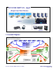
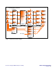
4 Application Diagrams HFRD-34.0 can be configured in a variety of application environments. Three possible applications are shown in Figures 1 through 3 below. DVI KVM SWITCH - App1 (2-Person Work Station) USER 2 USER 1 SHARED Figure 1. Typical application. DVI KVM SWITCH - App2 (4-Person Work Station) USER 1 USER 2 USER 3 USER 4 SHARED Figure 2. Typical application. Reference Design HFRD-34.0 (Rev.
DVI KVM SWITCH - App3 (Single User Work Station) USER 1 SHARED Figure 3. Typical application. 5 Functional Diagrams HFRD-34.
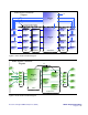
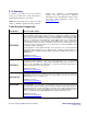
Video-Section Functional Diagram I2C 5 MAX4814 x2 5 5 5 Low-Speed Video Signals High-Speed Video Signals 8 DVI In1 8 DVI In2 8 DVI In3 8 DVI In4 MAX3208 x2 MAX3814 MAX3208 x2 DVI Out1 MAX3208 x2 MAX3814 MAX3208 x2 DVI Out2 MAX3208 x2 MAX3814 MAX3208 x2 DVI Out3 MAX3208 x2 MAX3814 MAX3208 x2 DVI Out4 ESD Equalizers MAX3845 x2 Switch/MUX ESD Figure 5. Video-section functional diagram.
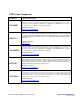
USB-Section Functional Diagram I2C 2 USB 1 4 MAX3207 USB2512 MAX3207 USB2512 2 USB 2 MAX4906 x8 MAX3208 USB HUB 2 2 - Port MAX3208 USB HUB 3 2 - Port USB HUB 4 2 - Port 4 MAX3207 USB2512 MAX3207 USB2513 MAX3208 HUB Controllers ESD 2 USB 4 USB HUB 1 2 - Port 4 2 USB 3 MAX3208 4 ESD Switches Data Power 2 MAX1558 2 MOSFETs x12 MAX1558 2 MAX1558 Power Switches 2 Main Supply MAX1558 Overcurrent Protection Figure 7. USB-section functional diagram. Reference Design HFRD-34.
6 IC Summary A summary of the ICs used in this reference design is provided below, along with links to additional information for each device. HFRD-34.0 demonstrates the operation of a small sample of Maxim’s digital and analog switches, digital video equalizers, power-management products, and audio drivers. For additional information about other Maxim products for this and many other applications, please visit: www.maxim-ic.com.
USB Section Components Part Number MAX4906F Functional Description The MAX4906F analog multiplexer combines the low on-capacitance (CON) and low onresistance (RON) necessary for high-performance switching applications. This device is designed for USB 2.0 Hi-Speed applications at 480Mbps. The MAX4906F also handles all the requirements for USB low- and full-speed signaling. Additional information: www.maxim-ic.
Audio Section Components Part Number MAX4550 Functional Description The MAX4550 serial-interface, programmable, dual 4x2 audio/video crosspoint switch is ideal for multimedia applications. It contains two identical crosspoint switch arrays, each with four inputs and two outputs. To improve off-isolation, the additional crosspoint inputs, SA and SB, can be used as shunts. The output is selectively programmable for clickless or regular mode operation.
Control, Power Management, and Miscellaneous Components Part Number Functional Description The ATMega48 is a low-power CMOS 8-bit microcontroller based on the AVR enhanced RISC architecture. By executing instructions in a single clock cycle, the ATMega48 achieves throughputs approaching 1 MIPS per MHz, allowing the system designer to optimize power consumption versus processing speed.
MAX1853 The MAX1853 monolithic, CMOS charge-pump voltage inverter in the ultra-small SC70 package features a low 15Ω output resistance, which permits loads up to 30mA with maximum efficiency. The MAX1853 is available with an operating frequency of 200kHz, allowing optimization of supply current or external component size. Small external components and micropower shutdown mode make this device ideal for both batterypowered and board-level voltage conversion applications. Additional information: www.
MAX3420 The MAX3420E contains the digital logic and analog circuitry necessary to implement a fullspeed USB peripheral compliant to USB specification rev 2.0. A built-in full-speed transceiver features ±15kV ESD protection and programmable USB connect and disconnect. An internal serial-interface engine (SIE) handles low-level USB protocol details such as error checking and bus retries. The MAX3420E operates using a register set accessed by an SPI™ interface that operates up to 26MHz.
CM 3 Default Sets the default configuration for the reference (Audio/Video/USB In1 to Audio/Video/USB Audio/Video/USB In2 to Audio/Video/USB Out2, etc.) CM 4 Demo Mode Puts the reference design into a demonstration mode. When in this mode, the controller will loop through the default and saved configurations at a preset time interval. This operation allows for automatic switching of the DVI and audio signals. Please note: The USB configuration is not switched in demo mode (only DVI and Audio).
The current volume selection is highlighted. ACM 2 HP2 Volume Allows the user to adjust headphone 2 output volume (1through 7). The current volume selection is highlighted. ACM 3 Main Menu Return to Main Menu ADVM 1 DVI1 Pre-Emph Allows the user to adjust DVI Out 1 preemphasis level between 0dB, 3dB, and 6dB. The preemphasis can be increased to improve signal integrity when using long cables between HFRD-34.0 and the monitor.
8 Schematics, Component List, and Layout Drawings The full schematics, component list, and PCB layout drawings are available to download in PDF format at: http://www.maximic.com/tools/other/appnotes/4232/4232_softwar e.zip. See sections 10 and 11 for additional details regarding the use of the schematics and layout drawings for new designs. 9 Gerber Files and Firmware The Gerber files and firmware assist design engineers in developing their projects, and are available to Maxim customers upon request.
compatibility of the reference design with a wider variety of DVI video cards. 11 Evaluation/Use Notes This reference design aids designers and is not intended to replace the entire design process. The designer should evaluate the reference design and modify it, as necessary, to meet the specification for a particular project. The designer should also carefully consider safety and EMI issues related to the specific application. 2. 0.5oz copper foil before platting. 3.
1312 Board Dimensions Figure 8. HFRD-34.0 Board dimensions (not to scale). Reference Design HFRD-34.0 (Rev.
DVI is a trademark of Digital Display Working Group (DDWG). FireWire is a registered trademark of Apple Computer, Inc. HDMI is a trademark of HDMI Licensing, LLC. InfiniBand is a registered trademark of InfiniBand Trade Association. MultiTRAK is a trademark of Standard Microsystems Corporation. PCI Express is a registered trademark of PCI-SIG Corp. SMBus is a trademark of Intel Corporation. SPI is a trademark of Motorola, Inc. TMDS is a registered trademark of Silicon Image, Inc. Reference Design HFRD-34.