
Specifications


Reference Design HFRD-25.2 (Rev.8; 01/09) Maxim Integrated Products
Page 6 of 42
Note 2: Time to reach 90% of steady-state value after burst enable is asserted. If required by the application
this delay can be reduced by the use of external components. See Section 9.2 for additional details.
Note 3: Time to fall below 10% of steady-state value after burst enable is de-asserted.
Note 4: Initialization time for the laser output to reach 80% of its final value. Time is from when the laser
driver enable pin has been asserted low (by POR or external control) to when the optical output reaches 80%
of its final value. The bias current must be programmed properly into the lookup table for the initial bias
current to reach the 80% point within the time specified. If the first burst of data occurs more than 600ns
after enable has been asserted low (by POR or external control), then the initialization time is zero.
Note 5: Time is from V
CC
reaching 2.7V to when the laser driver can be first enabled. The length of this time
can be adjusted in firmware.
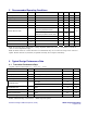
6.2 Receiver Performance Data
(Typical values are measured at: T
A
= +25
o
C, data rate = 1.25Gbps, 2
7
-1 PRBS pattern, V
CC
= +3.3V)
PARAMETER SYMBOL CONDITIONS TYP UNITS
Power Supply Current
Digital receiver only
76 mA
Overload P
AVGMAX
0 dBm
Sensitivity
P
AVGMIN
BER = 1E-12, with crosstalk -29 dBm
Assert -36.4
Loss of Signal, Note 1 LOS
De-assert -34.0
dBm
Loss of Signal Hysteresis 2.4 dB
Receiver Wavelength 1490 nm
Note 1: Range can be adjusted as desired using different component values.