
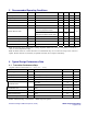
Specifications


Reference Design HFRD-25.2 (Rev.8; 01/09) Maxim Integrated Products
Page 4 of 42
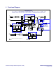
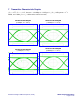
4 Functional Diagram
IN+
IN-
Laser
PECL / CML
Compatible Inputs
Modulation
and Bias
Outputs
MAX3643
TD-
TD+
OUT+
OUT-
HFRD-25.2
Low-Cost GEPON ONT/ONU Transceiver with
μ
C
Termination
TTL Termination
/ Level Shifter
BEN
PECL / CML
Compatible Inputs
BEN+
BEN-
1490nm
1310nm
Fiber
Monitor
Diode
BIAS+
V
CCT
OUT+
OUT-
Represents a controlled impedance transmission line
MAX3747
Signal
Detect /
Ref
Digital Offset
Correction Loop
CML
Ouput
RD-
RD+
100Ω Differential
100Ω Differential
Xponent
Diplexer
XP3-0063
PIN
V
CCR
TIA
LOS
Bias
Monitor / MD
SAMPLE and
Hold
VMSET
VBSET
MODSET
BIASSET
Atmel ATTiny24
Temp
Sensor
VCC
Compensated
PWM Outputs
with Pre-Charge
I2C
Compatible
Interface
Look-Up Table
for Instant On
Memory
ADC
BIASMON
RSSI (Optional)
MDMON
SDA
SCL
TX_DISABLE
BENOUT
EN
Figure 1. HFRD-25.2 functional diagram.