
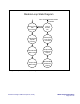
Specifications


Reference Design HFRD-25.2 (Rev.8; 01/09) Maxim Integrated Products
Page 38 of 42
13 SFF Module PIN Description
Component Name Function
1 MISO Used for ISP programming of the ATTiny24 microcontroller . This pin is also
internally connected to the MAX3643 BEN output.
2 GND Module ground. Note transmitter and receiver grounds are connected together on
the HFRD-25.2 PCB.
3 GND Module ground. Note transmitter and receiver grounds are connected together on
the HFRD-25.2 PCB.
4 NC No Connection
5 NC No Connection
6 GND Module ground. Note transmitter and receiver grounds are connected together on
the HFRD-25.2 PCB.
7 VCCR Receiver Power-Supply Connection (+3.3V)
8 LOS LOS asserts high if the received signal drops below the threshold set by R32 and
R33. When LOS asserts, the output will be squelched.
9 RD- Receiver (MAX3747) Inverted Data Output, AC-Coupled
10 RD+ Receiver (MAX3747) Nonnverted Data Output, AC-Coupled
11 VCCT Transmitter Power-Supply Connection (+3.3V)
12 GND Module ground. Note transmitter and receiver grounds are connected together on
the HFRD-25.2 PCB.
13 TDIS Transmitter Disable. When this pin is asserted high, the transmitter will be
disabled. TTL-compatible input
14 TD+ Transmitter (MAX3643) Nonnverted Data Input, DC-Coupled*
15 TD- Transmitter (MAX3643) Inverted Data Input, DC-Coupled*
16 GND Module ground. Note transmitter and receiver grounds are connected together on
the HFRD-25.2 PCB.
17 SCL Two-Wire Interface Clock Input
18 SDA Two-Wire Slave Data Interface
19
TX_BRST
Transmitter (MAX3643) Burst Enable Input, DC-Coupled, TTL-compatible*
TX_BRST must be asserted high if operating in continuous mode.
20
RESET
ATTiny24 Reset, Internally Pulled High. When this pin is asserted low, the μC will
reset to an initial state. This pin is also for ISP programming of the ATTiny24 μC.
*DC-Coupled I/O. Ensure that the DC voltage on these pins is compatible with the test equipment before
making any connections.