Reference Design: HFRD-25.2 Rev.8; 01/09 As of July, 2008 this reference design board is no longer available. Gerber files and schematics are available upon request.
Reference Design: Low-Cost GEPON SFF ONT with μC Table of Contents 1. Overview .................................................... 2 2. Obtaining Additional Information .............. 2 3. Reference Design Device Details ............... 3 4. Functional Diagram .................................... 4 5. Recommended Operating Conditions......... 5 6. Typical Design Performance Data.............. 5 7. Transmitter Characteristic Graphs.............. 7 8. Receiver Characteristic Graphs .................. 18 9.
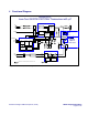
Reference Design Device Details HFRD-25.2 was engineered to meet the requirements of GEPON ONT/ONU transceiver applications (Figure 1) operating at 1.25Gbps burst upstream and 1.25Gbps continuous downstream. The design can also be easily adapted to other PON applications. The burst-mode upstream transmitter is implemented using the MAX3643 laser driver and the Atmel ATTiny24 microcontroller (μC). The downstream receiver consists of the MAX3747 limiting amplifier.
Functional Diagram HFRD-25.
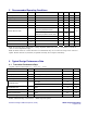
Recommended Operating Conditions PARAMETER Operating Ambient Temperature Supply Voltage SYMBOL TA CONDITIONS Note 1 MIN TYP 0 VCC 3.0 MAX +70 3.3 3.6 UNITS o C V Transmitter Data Rate 1.25 Gbps Digital Receiver Data Rate 1.25 Gbps Digital Receiver Input Power 0 dBm Bit 5 of Mode Register = 0 Continuously Repeated Interval 100 Bit 5 of Mode Register = 1 Continuously repeated interval, Note 2 500 Minimum Burst Off Time Continuously repeated interval, Note 2 4.
Note 2: Time to reach 90% of steady-state value after burst enable is asserted. If required by the application this delay can be reduced by the use of external components. See Section 9.2 for additional details. Note 3: Time to fall below 10% of steady-state value after burst enable is de-asserted. Note 4: Initialization time for the laser output to reach 80% of its final value.
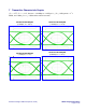
Transmitter Characteristic Graphs (TA = +25oC, VCC = +3.3V, data rate = 1244Mbps to 1.25Gbps, 11 ≥ ER ≤ 12dB, pattern = 27-1 PRBS, and -1dBm ≥ PAVG ≤ +1dBm unless otherwise noted.) OPTICAL EYE DIAGRAM (1.25Gbps, TA = +25oC) OPTICAL EYE DIAGRAM (1.25Gbps, TA = +70oC) OPTICAL EYE DIAGRAM (1.25Gbps, TA = 0oC) OPTICAL EYE DIAGRAM (1244Mbps, TA = +70oC) Reference Design HFRD-25.2 (Rev.
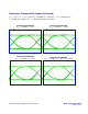
Transmitter Characteristic Graphs (continued) (TA = +25oC, VCC = +3.3V, data rate = 1244Mbps to 1.25Gbps, 11 ≥ ER ≤ 12dB, pattern = 27-1 PRBS, and -1dBm ≥ PAVG ≤ +1dBm unless otherwise noted.) OPTICAL EYE DIAGRAM (1244Mbps, 223-1 PRBS) OPTICAL EYE DIAGRAM (1244Mbps, 231-1 PRBS) OPTICAL EYE DIAGRAM (1244Mbps, Unfiltered) OPTICAL EYE DIAGRAM (622Mbps, 231-1 PRBS) Reference Design HFRD-25.2 (Rev.
Transmitter Characteristic Graphs (Continued) (TA = +25oC, VCC = +3.3V, data rate = 1244Mbps to 1.25Gbps, 11 ≥ ER ≤ 12dB, pattern = 27-1 PRBS, and -1dBm ≥ PAVG ≤ +1dBm unless otherwise noted.) OPTICAL EYE DIAGRAM (1.25Gbps, ER = 12.9dB) OPTICAL EYE DIAGRAM (1.25Gbps, ER = 13.5dB) OPTICAL EYE DIAGRAM (1.25Gbps, ER = 14.1dB) OPTICAL EYE DIAGRAM (1.25Gbps, ER = 14.7dB) Reference Design HFRD-25.2 (Rev.
Transmitter Characteristic Graphs (Continued) (TA = +25oC, VCC = +3.3V, data rate = 1244Mbps to 1.25Gbps, 11 ≥ ER ≤ 12dB, pattern = 27-1 PRBS, and -1dBm ≥ PAVG ≤ +1dBm unless otherwise noted.) OPTICAL EYE DIAGRAM (PAVG = +2.3dBm, TA = 0oC) OPTICAL EYE DIAGRAM (PAVG = +2.3dBm, TA = +25oC) OPTICAL EYE DIAGRAM (PAVG = +2.3dBm, TA = +70oC) OPTICAL EYE DIAGRAM (PAVG = +2.3dBm, TA = +70oC, ER = 13.3dB) Reference Design HFRD-25.2 (Rev.
Transmitter Characteristic Graphs (Continued) (TA = +25oC, VCC = +3.3V, data rate = 1244Mbps to 1.25Gbps, 11 ≥ ER ≤ 12dB, pattern = 27-1 PRBS, and -1dBm ≥ PAVG ≤ +1dBm unless otherwise noted.) POWER-ON RESET (Burst Mode, Slow Ramp) POWER-ON RESET (Burst Mode, Hot Plug) VCC VCC Optical Out Optical Out POWER-ON RESET (Continuous Mode, Slow Ramp) POWER-ON RESET (Continuous Mode, Hot Plug) VCC VCC Optical Out Reference Design HFRD-25.2 (Rev.
Transmitter Characteristic Graphs (continued) (TA = +25oC, VCC = +3.3V, data rate = 1244Mbps to 1.25Gbps, 11 ≥ ER ≤ 12dB, pattern = 27-1 PRBS, and -1dBm ≥ PAVG ≤ +1dBm unless otherwise noted.) INITIALIZATION TIME (Continuous Mode) VCC DISABLE PICTURE (Continuous Mode) Zoom Out 600ns Zoom In Optical Out INITIALIZATION TIME (Burst Mode, First Four Bursts After POR, First Burst Occurs More than 600ns After POR) Reference Design HFRD-25.2 (Rev.
Transmitter Characteristic Graphs (continued) (TA = +25oC, VCC = +3.3V, data rate = 1244Mbps to 1.25Gbps, 11 ≥ ER ≤ 12dB, pattern = 27-1 PRBS, and -1dBm ≥ PAVG ≤ +1dBm unless otherwise noted.) INITIALIZATION TIME (Burst Mode, First Burst After POR) Reference Design HFRD-25.2 (Rev.
Transmitter Characteristic Graphs (continued) (TA = +25oC, VCC = +3.3V, data rate = 1244Mbps to 1.25Gbps, 11 ≥ ER ≤ 12dB, pattern = 27-1 PRBS, and -1dBm ≥ PAVG ≤ +1dBm unless otherwise noted.) INITIALIZATION TIME (Burst Mode, Burst Several Seconds After POR. Cursors Shown in Same Location as Previous Picture (First Burst After POR) to Give a Reference of the Change.) Reference Design HFRD-25.2 (Rev.
Transmitter Characteristic Graphs (continued) (TA = +25oC, VCC = +3.3V, data rate = 1244Mbps to 1.25Gbps, 11 ≥ ER ≤ 12dB, pattern = 27-1 PRBS, and -1dBm ≥ PAVG ≤ +1dBm unless otherwise noted.) INITIALIZATION TIME (Burst Mode, First Burst After Disable then Re-EnableCursors Shown in Same Location as Previous Two Pictures to Give a Reference of the Change.) Reference Design HFRD-25.2 (Rev.
Transmitter Characteristic Graphs (continued) (TA = +25oC, VCC = +3.3V, data rate = 1244Mbps to 1.25Gbps, 11 ≥ ER ≤ 12dB, pattern = 27-1 PRBS, and -1dBm ≥ PAVG ≤ +1dBm unless otherwise noted.) OPTICAL BURST ON DIAGRAM (10ns/div) OPTICAL BURST OFF DIAGRAM (1ns/div) TRANSMITTER SUPPLY CURRENT (Transmitter Only, Includes Laser Current) EXTINCTION RATIO vs. SUPPLY VOLTAGE (Shows PWM Compensation of Modulation) 14 120 13.
Transmitter Characteristic Graphs (continued) (TA = +25oC, VCC = +3.3V, data rate = 1244Mbps to 1.25Gbps, 11 ≥ ER ≤ 12dB, pattern = 27-1 PRBS, and -1dBm ≥ PAVG ≤ +1dBm unless otherwise noted.) AVERAGE POWER (With Tracking Error Compensation) 2 2 1.5 1.5 1 1 Average Power (dBm) Average Power (dBm) AVERAGE POWER (With No Tracking Error Compensation) 0.5 0 -0.5 -1 0.5 0 -0.5 -1 -1.5 -1.
8 Receiver Characteristic Graphs (TA = +25oC, VCC = +3.3V, unless otherwise noted.) DATA OUTPUT DIAGRAM (1.25Gbps, ≈ -29dBm Input) DATA OUTPUT DIAGRAM (1.25Gbps, ≈ -5dBm Input) Reference Design HFRD-25.2 (Rev.8; 01/09) DATA OUTPUT DIAGRAM (1.25Gbps, ≈ -20dBm Input) DATA OUTPUT DIAGRAM (1.
Receiver Characteristic Graphs (continued) (TA = +25oC, VCC = +3.3V, unless otherwise noted.) LOS ASSERT/DEASSERT (Note: Levels Can Be Adjusted as Desired) 120 -30 112 -31 104 -32 96 -33 Input Level (dBm) Supply Current (mA) RECEIVER SUPPLY CURRENT 88 80 72 64 De-Assert -34 -35 Assert -36 -37 56 -38 48 -39 -40 40 0 10 20 30 40 50 60 0 70 10 20 o 70 BIT ERROR RATIO 1.E-03 1.E-03 1.E-04 1.E-04 1.E-05 1.
9 Application Information 9.1 Design Details HFRD-25.2 provides PON modules designers with a simple, low-cost, high-performance and feature-rich reference design for GEPON ONT/ONU modules. The design can also be used as a reference for GPON and BPON designs as many of the features and components are compatible with those standards. The HFRD-25.2 reference design also includes the complete and documented firmware code for the ATMEL ATTiny24 μC, which is used in the design.
10 Controls/Features 10.1 Overview Through the use of a low-cost microcontroller, HFRD-25.2 provides many control options and monitoring features. These features and monitors are explained in the sections that follow. 10.2 Modes of Operation The HFRD-25.2 design can operate in a variety of different modes (burst mode, continuous mode, open loop, etc.). The mode of operation is set by byte 00 (MODE) located in EPROM memory. Each bit in byte 00 corresponds to a different feature or mode of operation.
10.3 Memory Summary The ATTiny24 microcontroller incorporates 128bytes of SRAM and 128bytes of EEPROM. Tables 2 and 3 list the EEPROM and SRAM memory allocations. Table 2: EEPROM Memory (00h to 7Fh, Hexadecimal Is Indicated by the Trailing “h”.) Byte Name/Definition 00h MODE: Mode of Operation Control Byte (See Table 1) 01h MODSET: Stores the calibrated modulation PWM output value which relates to the desired modulation output current (Section 10.4).
0Eh SupplyO: Supply voltage offset for VCC calibration routine. See Section 10.6 for additional details. 0Fh Unused memory location. 10h Instant-On Lookup Table values. Each location holds the initial bias current value for a given temperature from -40oC to +100oC, where address 10h corresponds to -40oC and 33h corresponds to +100oC to 33h 34h to Vendor EEPROM for module identification, etc. 7Fh Table 3: SRAM Memory (60h to E0h) Byte Name/Definition 60h SRAM_OFFSET: Memory control byte.
7Fh to Microcontroller Stack SRAM AFh B0h to Program Accessed SRAM E0h 10.4 PWM Outputs Two 8-bit PWM outputs from the ATTiny24 are used to set the bias and modulation currents of the MAX3643 laser driver. By passing the PWM output through a lowpass filter and resistive divider, a low-noise, digitally-adjustable voltage is generated. The voltage output is given by: ⎛ 255 − PWMV ⎞ ⎛ 5.1k ⎞ VOUT = VCC ⋅ ⎜ ⎟⋅⎜ ⎟ 255 ⎝ ⎠ ⎝ 20.
10.6 VCC Calibration HFRD-25.2 provides a monitor of the supply voltage. To calibrate the VCC monitor: 1. Set the supply voltage of the module to 3.3V (voltage at the VCC pin of the module). 2. Adjust the SupplyO value (EEPROM 0Eh, typical value = 1Ch (28)), until the digital value reported in SupplyVH and SupplyVL (SRAM 70h, 71h) is equal to D7h (215). Please note that the power or reset signal should be cycled after each change in the SupplyO value.
operating in continuous-mode operation, the initialization time is approximately 600ns from power-on. 10.9 K-Factor Modulation Compensation HFRD-25.2 includes a type of K-Factor modulation compensation for adjusting the modulation current with changing temperature. The amount of compensation (KC) applied equals: ⎛ KFactorSH ⎞ ⎛ IBiasV ( SRAM 75h,76h ⎞ KC = ⎜ ⎟ ⎟⋅⎜ 100 4 ⎝ ⎠ ⎝ ⎠ KC is a digital value which is then applied to the modulation PWM value to increase the modulation current output.
11 Firmware all memory read and write functions through the two-wire interface. 11.1 Overview 6. MemFunctions.ams - Includes simple routines for pulling data from EEPROM and setting up the various registers and memory banks. The sections below provide a brief overview of the firmware files and state diagrams of the main sections of the firmware implemented in the reference design. 11.2 Compiler The firmware for HFRD-25.2 was developed using Atmel AVR studio 4.12, Service Pack 3, Build 490.
Top-Level State Diagram RESET Interrupt Routines Figure 4 Figure 5 Figure 9 Initialize/ Configure PortA, PortB Two-Wire Interface Monitor Diode Sample APC Loop / Modulation Comp. Figure 6 Initialize Interrupts And Two-Wire Interface EEPROM Write TDIS Pin Change Configure APC Loop Load EEPROM Figure 8 Enable Output Figure 3 Initialize Disable Loop Update Monitors/ Memory PWM Precharge Check Operation Mode Open-Loop Mode States in bold are shown in additional detail in subsequent Figures.
Initialize PWM and Precharge State Diagram Configure PWM Mode Set Boost value if Precharge is Enabled Increase PWM Value (Decrease Voltage) Compare New Value to Final Desired Value Calculate Bias and Mod PWM Values Output New Value if < Final Desired Value Sample Temp Sample Temp Bias VCC RSSI Bias VCC RSSI Calculate Bias and Mod PWM Values Set PWM to Output a High Voltage Loop 12x Loop Sample Temp Bias VCC RSSI Calculate Bias and Mod PWM Values Output Calibrated Values Figure 3.
Monitor Diode Sample State Diagram Check For Continuous or Burst Mode Check if BurstOff Interrupt Occurred Burst Off < 5uS Exit with No APC Loop Update Burst Off > 5uS Finish A/D Disable BurstOff Counter Switch A/D Input as Needed Store Result in Memory BENOUT = 0 Sample BENOUT BENOUT = 1 Burst Mode Burst On< 500ns Exit with No APC Loop Update Init. Burst-Off Counter Go to APC Loop BENOUT = 1 Cont. Mode Check On Time (If Enabled) Burst On > 500ns Start A/D Figure 4.
APC Loop and ModulationCompensation State Diagram Exit Update Mod Output Init APC Loop Counter Compare Value to Calibration Value Greater Than Equal Call Mod Integrator Less Than Inc Integrator Counter Dec Integrator Counter Call VCC Comp Compare Counter Value to 0 Apply Mod Temperature Comp Counter = Terminal Count Compare Counter Value to Terminal Count Not = Counter = 0 Inc PWM Value Apply Mod K-Factor Comp Dec PWM Value Bit 0 = 1 Reset Counter Output New Value Dec Control Counter B
Update Monitors and Memory State Diagram Quick Conversion to Clear Prev. Temp Conversion/ Update Bias Conversion/ Update RSSI Conversion/ Update Mode Bit 2 = 0 Exit VCC Conversion/ Update Mode Bit 2 = 1 Quick Conversion to Clear Prev. VCC Conversion/ Update Read EEPROM 01h to 0Ah Update SRAM Registers Exit Figure 6. Simplified update monitors and memory state diagram. Reference Design HFRD-25.2 (Rev.
Open-Loop State Diagram Jump to Disable Loop Disabled Monitor Enable Pin Enabled Monitor Diode A/D Conversion Output New Modulation Output Call Monitor Update Routine Calculate New Modulation Output Calculate New Output New Bias Value Bias Value Figure 7. Simplified open-loop state diagram. Reference Design HFRD-25.2 (Rev.
Disable-Loop State Diagram Go to Check Operation Mode Enabled Monitor Diode Disabled A/D Conversion Check Enable Pin Call Monitor Update Routine Reset APC Loop Time Constant Calculate New Bias Value Output New Modulation Output Output New Bias Value Calculate New Modulation Output Figure 8. Simplified disable-loop state diagram. Reference Design HFRD-25.2 (Rev.
Simplified Two-Wire Interface State Diagram Buffer Full Interrupt Start Condition Interrupt Get Dev Address/ Check Address Address Match ACK Load Next State (R/W) Address Mismatch Do Nothing; Wait for Next Start Condition Interrupt Get Data Address Read Write ACK Init Buffer Full Interrupt Output Data Inc Address Value NACK or Stop Get Data Send ACK ACK Wait for Next Start Condition Interrupt Write Data to Address, Inc Addr. Value NACK or Stop Figure 9.
12 Evaluation Quick Start 12.1 Evaluation Notice The HFRD-25.2 reference design has DC-coupled I/O (see Sections 13 and 15) and a large optical output signal (approximately -1.0dBm to +1.0dBm). When evaluating the HFRD-25.2 reference design, ensure that proper connections are made to the test equipment. Also check that all signal levels are within the proper range (common-mode, differential swing, optical input/output power, etc.) to avoid damage to the test equipment or reference design.
Figure 10. HFRD-25.2 graphical user interface. Reference Design HFRD-25.2 (Rev.
13 SFF Module PIN Description Component Name Function 1 MISO Used for ISP programming of the ATTiny24 microcontroller . This pin is also internally connected to the MAX3643 BEN output. 2 GND Module ground. Note transmitter and receiver grounds are connected together on the HFRD-25.2 PCB. 3 GND Module ground. Note transmitter and receiver grounds are connected together on the HFRD-25.2 PCB.
HFRD-25.2 TOP View MS MS 1 10 MAX3747 ATTiny24 Xponent Diplexer MAX3643 MS 11 20 MS Figure 11. HFRD-25.2 top view. 14 Component List DESIGNATION QTY C3 1 C5, C9, C21, C22 4 C8 1 C10–C12, C14, C15, C29–C32, C35, C39, C40, C103 13 C13 1 C17 1 C36 1 L1, L2, L14 3 L3, L5, L15 3 R1, R20 R2 R5 R6, R23, R25 R7 R8, R9 2 1 2 3 1 2 DESCRIPTION 0.22μF ± 10%, 10V Ceramic Capacitor (0402) 1μF ± 20%, 10V Ceramic Capacitor (0402) 39pF ± 10% 50V Ceramic Capacitor (0402) 0.
15 Schematics Figure 12. HFRD-25.2 schematic. Reference Design HFRD-25.2 (Rev.
16 Board Layout Figure 13. Component placement guide. Figure 14. Board layout, layer 1. Figure 15. Board layout, layer 2. Reference Design HFRD-25.2 (Rev.
Figure 16. Board layout, layer 3. Figure 17. Board layout, layer 4. 17 Layer Profile The HFRD-25.2 reference-design board includes controlled-impedance transmission lines. The layer profile is based on the following assumptions: 1. Dielectric material is FR-4 with a dielectric constant of ~ 4.5 2. 1oz copper foil Single Ended Coupled A N.A. 8mil B >50mil 10mil C 8mil 8mil D As Needed As Needed PREPREG A B A C D CORE C PREPREG Figure 18. Layer profile.