
User`s guide


DS87C530/DS83C530 EPROM/ROM Microcontrollers with Real-Time Clock
34 of 45
DC ELECTRICAL CHARACTERISTICS (continued)
(V
CC
= 4.5V to 5.5V, T
A
= -40°C to +85°C.)
PARAMETER SYMBOL MIN TYP MAX UNITS NOTES
Input Leakage Port 0, EA, Pins, I/O Mode
I
L
-10 +10
A
13
Input Leakage Port 0, Bus Mode
I
L
-300 +300
A
14
RST Pulldown Resistance
R
RST
50 200
k
Note 1:
Storage temperature is defined as the temperature of the device when V
CC
= 0V and V
BAT
= 0V. In this state, the contents of
SRAM are not battery backed and are undefined.
Note 2:
All parameters apply to both commercial and industrial temperature operation unless otherwise noted.
Note 3:
All voltages are referenced to ground.
Note 4:
Active current measured with 33MHz clock source on XTAL1, V
CC
= RST = 5.5V, other pins disconnected.
Note 5:
Idle mode current measured with 33MHz clock source on XTAL1, V
CC
= 5.5V, RST at ground, other pins disconnected.
Note 6:
Stop mode current measured with XTAL1 and RST grounded, V
CC
= 5.5V, all other pins disconnected.
Note 7:
V
CC
= 0V, V
BAT
= 3.3V. 32.768kHz crystal with 12.5pF load capacitance between RTCX1 and RTCX2 pins. RTCE bit set to 1.
Note 8:
RST = V
CC
. This condition mimics operation of pins in I/O mode. Port 0 is tri-stated in reset and when at a logic high state during
I/O mode.
Note 9:
During a 0-to-1 transition, a one-shot drives the ports hard for two clock cycles. This measurement reflects port in transition
mode.
Note 10:
When addressing external memory. This specification only applies to the first clock cycle following the transition.
Note 11:
This is the current required from an external circuit to hold a logic low level on an I/O pin while the corresponding port latch bit is
set to 1. This is only the current required to hold the low level; transitions from 1 to 0 on an I/O pin will also have to overcome the
transition current.
Note 12:
Ports 1, 2, and 3 source transition current when being pulled down externally. It reaches its maximum at approximately 2V.
Note 13:
0.45 < V
IN
< V
CC
. RST = V
CC
. This condition mimics operation of pins in I/O mode.
Note 14:
0.45 < V
IN
< V
CC
. Not a high-impedance input. This port is a weak address holding latch in Bus Mode. Peak current occurs near
the input transition point of the latch, approximately 2V.
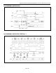
TYPICAL I
CC
vs. FREQUENCY