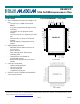
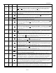
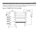
DS5001FP 128k Soft Microprocessor Chip www.maxim-ic.com FEATURES § § § PIN ASSIGNMENT (Top View) BA11 P0.5/AD5 PE1 P0.6/AD6 BA10 P0.7/AD7 CE1 NC CE1N BD7 ALE BD6 PSEN BD5 P2.
DS5001FP DESCRIPTION The DS5001FP 128k soft microprocessor chip is an 8051-compatible microprocessor based on NV RAM technology and designed for systems that need large quantities of nonvolatile memory. It provides full compatibility with the 8051 instruction set, timers, serial port, and parallel I/O ports. By using NV RAM instead of ROM, the user can program and then reprogram the microprocessor while in-system.
DS5001FP Figure 1.
DS5001FP PIN DESCRIPTION 80-PIN MQFP 11, 9, 7, 5, 1, 79, 77, 75 15, 17, 19, 21, 25, 27, 29, 31 49, 50, 51, 56, 58, 60, 64, 66 44-PIN MQFP SIGNAL DESCRIPTION 31 (P0.5) P0.0–P0.7 General-Purpose I/O Port 0. This port is open-drain and cannot drive a logic 1. It requires external pullups. Port 0 is also the multiplexed expanded address/data bus. When used in this mode, it does not require pullups. 44 (P1.3) P1.0–P1.7 General-Purpose I/O Port 1 N/A P2.0–P2.7 General-Purpose I/O Port 2.
DS5001FP 33, 35, 37 71, 69, 67, 65, 61, 59, 57, 55 28, 26, 24, 23, 21, 20, 19, 18 BD7–0 10 37 R/ W 74 29 CE1 72 N/A CE1N 2 33 CE2 63 22 CE3 62 N/A CE4 78 N/A PE1 3 N/A PE2 22 N/A PE3 23 N/A PE4 32 N/A PROG 42 N/A VRST 43 N/A PF 14 40 MSEL 73 9 and A15 respectively. NC Byte-Wide Data-Bus Bits 7–0. This 8-bit, bidirectional bus is combined with the nonmultiplexed address bus (BA14–0) to access NV SRAM. Decoding is performed on CE1 and CE2 .
DS5001FP INSTRUCTION SET The DS5001FP executes an instruction set that is object code-compatible with the industry standard 8051 microcontroller. As a result, software development packages such as assemblers and compilers that have been written for the 8051 are compatible with the DS5001FP. A complete description of the instruction set and operation are provided in the Secure Microcontroller User’s Guide. Also note that the DS5001FP is embodied in the DS2251T module.
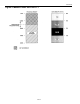
DS5001FP Figure 3. MEMORY MAP IN PARTITIONABLE MODE (PM = 0) Note: Partitionable mode is not supported when MSEL pin = 0 (128kB mode).
DS5001FP Figure 4.
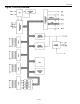
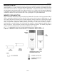
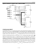
DS5001FP Figure 5 illustrates a typical memory connection for a system using a 128kB SRAM. Note that in this configuration, both program and data are stored in a common RAM chip Figure 6 shows a similar system with using two 32kB SRAMs. The byte-wide address bus connects to the SRAM address lines. The bidirectional byte-wide data bus connects the data I/O lines of the SRAM. Figure 5.
DS5001FP Figure 6. DS5001FP CONNECTION TO 64k x 8 SRAM POWER MANAGEMENT The DS5001FP monitors VCC to provide power-fail reset, early warning power-fail interrupt, and switch over to lithium backup. It uses an internal bandgap reference in determining the switch points. These are called VPFW, VCCMIN, and VLI, respectively. When VCC drops below VPFW, the DS5001FP performs an interrupt vector to location 2Bh if the power-fail warning was enabled. Full processor operation continues regardless.
DS5001FP ABSOLUTE MAXIMUM RATINGS* Voltage Range on Any Pin Relative to Ground Voltage Range on VCC Related to Ground Operating Temperature Range Storage Temperature Range1 Soldering Temperature -0.3V to (VCC + 0.5V) -0.3 °C to 6.0°C -40°C to +85°C -55°C to +125°C See IPC/JEDEC J-STD-020A * This is a stress rating only and functional operation of the device at these or any other conditions above those indicated in the operation sections of this specification is not implied.
DS5001FP DC CHARACTERISTICS (continued) PARAMETER Input Leakage Current 0.
DS5001FP AC CHARACTERISTICS EXPANDED BUS MODE TIMING SPECIFICATIONS (TA = 0°C to +70°C; VCC = 5V ±10%) # 1 2 3 4 PARAMETER Oscillator Frequency ALE Pulse Width Address Valid to ALE Low Address Hold After ALE Low ALE Low to Valid Instruction In 5 6 7 8 9 10 11 12 13 14 15 16 17 18 19 20 21 22 23 24 25 26 27 SYMBOL 1/ tCLK tALPW tAVALL tAVAAV at 12MHz at 16MHz tALLVI tALLPSL tPSPW ALE Low to PSEN Low PSEN Pulse Width PSEN Low to Valid Instruction In at 12MHz at 16MHz Input Instruction Hold After PSEN Go
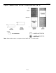
DS5001FP EXPANDED PROGRAM-MEMORY READ CYCLE EXPANDED DATA-MEMORY READ CYCLE 14 of 26
DS5001FP EXPANDED DATA-MEMORY WRITE CYCLE 15 of 26
DS5001FP AC CHARACTERISTICS (continued) EXTERNAL CLOCK DRIVE # (TA = 0°C to +70°C; VCC = 5V ±10%) PARAMETER External Clock-High Time 28 SYMBOL MIN MAX UNITS at 12MHz at 16MHz tCLKHPW 20 15 ns at 12MHz at 16MHz tCLKLPW 20 15 ns at 12MHz at 16MHz tCLKR 20 15 ns at 12MHz at 16MHz tCLKF 20 15 ns External Clock-Low Time 29 External Clock-Rise Time 30 External Clock-Fall Time 31 EXTERNAL CLOCK TIMING 16 of 26
DS5001FP AC CHARACTERISTICS (continued) POWER CYCLE TIME # 32 33 34 PARAMETER Slew Rate from VCCMIN to VLI Crystal Startup Time Power-On Reset Delay (TA = 0°C to +70°C; VCC = 5V ±10%) SYMBOL tF tCSU tPOR POWER CYCLE TIMING 17 of 26 MIN 130 MAX (Note 9) 21,504 UNITS µs tCLK
DS5001FP AC CHARACTERISTICS (continued) SERIAL PORT TIMING, MODE 0 # 35 PARAMETER Serial-Port Clock-Cycle Time 36 (TA = 0°C to +70°C; VCC = 5V ±10%) SYMBOL tSPCLK 12tCLK UNITS µs Output-Data Setup to Rising-Clock Edge tDOCH 10tCLK - 133 ns 37 Output-Data Hold After Rising-Clock Edge tCHDO 2tCLK - 117 ns 38 Clock-Rising Edge to Input-Data Valid tCHDV 39 Input-Data Hold After Rising-Clock Edge tCHDIV SERIAL PORT TIMING, MODE 0 18 of 26 MIN MAX 10tCLK - 133 0 ns ns
DS5001FP AC CHARACTERISTICS (continued) BYTE-WIDE ADDRESS/DATA BUS TIMING (TA = 0°C to +70°C; VCC = 5V ±10%) # 40 41 42 43 44 45 46 47 48 49 50 51 PARAMETER Delay to Byte-Wide Address Valid from CE1 , CE2 , or CE1N Low During Op Code Fetch Pulse Width of CE 1-4, PE 1-4 or CE1N Byte-Wide Address Hold After CE1 , CE2 , or CE1N High During Op Code Fetch Byte-Wide Data Setup to CE1 , CE2 , or CE1N High During Op Code Fetch Byte-Wide Data Hold After CE1 , CE2 or CE1N High During Op Code Fetch Byte-Wide Address
DS5001FP BYTE-WIDE BUS TIMING RPC AC CHARACTERISTICS, DBB READ (TA = 0°C to +70°C; VCC = 5V ±10%) # 54 55 56 57 58 59 PARAMETER CS , A0 Setup to RD CS , A0 Hold After RD RD Pulse Width CS , A0 to Data-Out Delay RD to Data-Out Delay RD to Data-Float Delay SYMBOL tAR tRA tRR tAD tRD tRDZ 20 of 26 MIN 0 0 160 0 MAX 130 130 85 UNITS ns ns ns ns ns ns
DS5001FP RPC AC CHARACTERISTICS, DBB WRITE (TA = 0°C to +70°C; VCC = 5V ±10%) # 60 61A 61B 62 63 64 PARAMETER CS , A0 Setup to WR CS , Hold After WR A0, Hold After WR WR Pulse Width Data Setup to WR Data Hold After WR SYMBOL tAW tWA tWA tWW tDW tWD AC CHARACTERISTICS, DMA # 65 66 67 68 DACK RD or DACK RD or PARAMETER to WR or RD WR to DACK to Data Valid WR to DRQ Cleared PARAMETER PROG Low to Active PROG High to Inactive MAX UNITS ns ns ns ns ns ns (TA = 0°C to +70°C; VCC = 5V ±10%) SYMBOL tACC
DS5001FP RPC TIMING MODE 22 of 26
DS5001FP NOTES: All parameters apply to both commercial and industrial temperature operation unless otherwise noted. 1) All voltages are referenced to ground. 2) Maximum operating ICC is measured with all output pins disconnected; XTAL1 driven with tCLKR, tCLKF = 10ns, VIL = 0.5V; XTAL2 disconnected; RST = PORT0 = VCC, MSEL = VSS. 3) Idle mode, IIDLE, is measured with all output pins disconnected; XTAL1 driven with tCLKR, tCLKF = 10ns, VIL = 0.5V; XTAL2 disconnected; PORT0 = VCC, RST = MSEL = VSS.
DS5001FP 80-PIN MQFP DIM MM MIN MAX A 3.40 A1 0.25 A2 2.55 2.87 B 0.30 0.50 C 0.13 0.23 D 23.70 24.10 D1 19.90 20.10 E 17.70 18.10 E1 13.90 14.10 e 0.80 BSC L 0.65 0.
DS5001FP 44-PIN MQFP 25 of 26
DS5001FP REVISION HISTORY The following represent the key differences between 112795 and 073096 version of the DS5001FP data sheet. Please review this summary carefully. 1) Change VCC02 specification from VLI - 0.5 to VLI - 0.65 (PCN F62501). 2) Update mechanical specifications. The following represent the key differences between 073096 and 111996 version of the DS5001FP data sheet. Please review this summary carefully. 1) Change VCC01 from VCC - 0.3 to VCC - 0.35.