
Owner's manual


6-18
Ultra-High-Speed Flash
Microcontroller User’s Guide
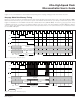
Page Mode 1 Data Memory Timing–Pages 1:0 = 01b (Two Cycles)
Figure 6-15 below shows execution of back-to-back MOVX instructions from internal flash memory. A stretch value = 0 (MD2:0 = 000b)
has been assigned. Note that the internal memory cycles consist of one system clock while the external memory cycles consist of two
system clocks (page hit) or four system clocks (page miss).
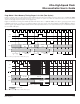
Figure 6-16 illustrates the timing of the MOVX operation with stretch value = 1 (MD2:0 = 001b). The stretch cycle (four system clocks)
is distributed as follows: one system clock added for address setup, two system clocks being added to the RD or WR pulse duration,
and one system clock added for address/data hold. For subsequent stretch values of 2 or 3, the full stretch cycle is added to the dura-
tion of the RD or WR pulse.
SYSCLK
ALE
PSEN
PORT2
PORT0
WR/RD
MOVX #1
MSB
MOVX #1
LSB
MOVX #2
MSB
MOVX
DATA
MOVX
DATA
MOVX #2
LSB
MOVX
#1
MOVX
#2
INSTRUCTIONSINST
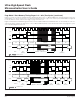
MOVX #1 DATA ACCESS
(PAGE MISS)
MOVX #2 DATA ACCESS
(PAGE MISS)
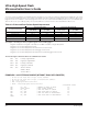
SYSCLK
ALE
PSEN
PORT2 MOVX MSB MOVX LSB
MOVX DATAPORT0
WR/RD
MOVX INST INSTRUCTIONS
MOVX DATA ACCESS
(PAGE MISS + 1 STRETCH CYCLE)
= STRETCH CYCLE
Figure 6-16. Two-Cycle Page Mode 1: MOVX (Three Cycles)
Figure 6-15. Two-Cycle Page Mode 1: MOVX (Two Cycles)
Maxim Integrated