
Owner's manual


5-14
Ultra-High-Speed Flash
Microcontroller User’s Guide
Page Mode 1 External Timing—Pages 1:0 = 00b (One Cycle) (continued)
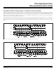
Figure 5-19 illustrates the JBC bit, rel (3 bytes, four cycles) instruction for the case where the tested bit is clear and the jump is not
taken. Note that one stall cycle must be inserted since the cycle count exceeds the byte count by one. The RET (1 byte, three cycles)
instruction that follows requires insertion of two stall cycles. In this example, the return address is on a different 256-byte page than the
RET instruction, thus resulting in a page-miss memory cycle. The MOV direct, #data (3 bytes, three cycles) executed next provides an
example of an instruction not requiring any stall cycles.
Figure 5-20 shows the same JBC bit, rel instruction for the case where the tested bit is set and the jump is taken. Since the bit must
be cleared and involves one of the special registers (PSW, SP, DPS, IE, EIE, IP0, IP1, EIP0, EIP1), a fifth memory cycle is required. For
this example, the jump taken by the JBC instruction crosses a 256-byte page boundary, while the RET instruction stays on the same
page.
SYSCLK
ALE
PSEN
PORT2
P
O
RT0
10
D1 1D
H
IT
H
IT
M
ISS
J
BC PSW.1, $+20h
LSB
s
tall
H
IT
H
IT
H
IT
s
tall
s
tall
22 75 90 55
M
ISS
H
IT
H
IT
H
IT
M
OV P1,#55h
s
tall
R
ET
Figure 5-20. One-Cycle Page Mode 1: (Page Miss) – JBC Bit, Rel (Five Cycles) – (Page Miss) – RET – MOV Direct, Data
R
ET
SYSCLK
ALE
PSEN
PORT2
PORT0
10
D1 1D
H
IT
H
IT
M
ISS
J
BC PSW.1, $+20h
LSB
22
s
tall
H
IT
H
IT
H
IT
s
tall
s
tall
LSB
75 90
55
H
IT
H
IT
H
IT
H
IT
M
OV P1,#55h
M
ISS
Figure 5-19. One-Cycle Page Mode 1: (Page Miss) – JBC Bit, Rel (Four Cycles)) – RET – (Page Miss)– MOV Direct, Data
Maxim Integrated