
Owner's manual


5-13
Page Mode 1 External Timing—Pages 1:0 = 00b (One Cycle)
The page mode 1 external bus structure multiplexes port 2 to provide the address MSB and LSB. Data transactions occur exclusive-
ly on port 0. ALE is used to latch the address MSB only when needed, and PSEN serves as the enable for external program memory.
Note that the one-cycle configuration differs slightly from the two-cycle and four-cycle configurations of the page mode 1 bus structure
in that PSEN does not toggle for consecutive page hits, but stays in the active-low state. To invoke one-cycle page mode 1 operation,
the PAGES 1:0 bits must be set to 00b, followed by the setting of the PAGEE bit. In the 1-cycle Page Mode 1 configuration, a page-hit
memory cycle is one system clock in length, while the page-miss memory cycle requires two system clocks.
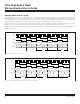
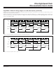
In Figure 5-17, the CLR C (1 byte, one cycle) instruction fetch occurs during a page-miss memory cycle, followed by the RRC A instruc-
tion (1 byte, 1 cycle) instruction fetch during a page-hit memory cycle. The MUL AB (1 byte, nine cycles) instruction, which occurs
next, requires that the program counter be stalled for eight additional memory cycles so that execution can complete. In a similar fash-
ion, the DA A (1 byte, two cycles) instruction, which follows the multiply, requires that one stall be inserted.
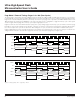
Figure 5-18 illustrates the memory cycle dependence of some direct instructions on the SFR addressed. The ORL direct, A is shown
for cases where P1 and IE are being addressed.
SYSCLK
ALE
PSEN
PORT 2
PORT 0
MISS HIT HIT HIT HIT HIT HIT HIT HIT HIT HITHIT
00
45
A89045
HIT HIT
STALL
NOP
LSB
MUL AB
ORL, P1, A
Figure 5-18. One-Cycle Page Mode 1: (Page Miss) – ORL Direct, A (Two Cycles) – ORL, A (Three Cycles) – NOP
SYSCLK
ALE
PSEN
PORT 2
PORT 0
MISS HIT HIT HITHIT
00D4A413C3
HIT STALLSTALLS
CLR C RRC A NOP
LSB ADDRESS
DA AMUL AB
Figure 5-17. One-Cycle Page Mode 1: (Page Miss) – CLR C – MUL AB – DA A – NOP
Ultra-High-Speed Flash
Microcontroller User’s Guide
Maxim Integrated