
Owner's manual


5-7
SYSCLK
ALE
PSEN
PORT 2
PORT 0
LSBLSB LSB
INC DPL
LSB LSB058205 86 E0 E0
MSB ADDRESS
INC DPS
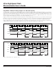
Figure 5-6. Nonpage Mode: INC Direct (Two Cycles) – INC Direct (Three Cycles)
SYSCLK
ALE
PSEN
PORT 2
PORT 0
MSB ADDRESS
LSB LSB
DA A RRC A
LSB LSBD4 13 13
MSB ADDRESS
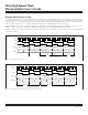
Figure 5-5. Nonpage Mode: DA A – RRC A
Ultra-High-Speed Flash
Microcontroller User’s Guide
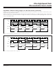
Nonpage Mode External Timing
The ultra-high-speed flash microcontroller defaults to a nonpage mode external memory interface. The nonpage mode bus structure
requires four system clock cycles per memory cycle. In the nonpage mode, the ALE signal latches the address LSB on each program
fetch. When the cycle count of an instruction exceeds the byte count, “dummy” fetches are performed each cycle until instruction exe-
cution is complete. Figures 5-5 to 5-8 demonstrate the basic timing for nonpage mode instruction execution.
Figure 5-5 shows the execution of the DA A instruction (1 byte, two cycles) followed by execution of the RRC A (1 byte, one cycle)
instruction. When a code fetch is made from a different 256-byte page, the new address MSB is presented on port 2.
Figure 5-6 shows the execution of the INC direct instruction (2 bytes) for the cases where an extra memory cycle is not (INC DPL) and
is (INC DPS) required.
Maxim Integrated