
Owner's manual


4-23
RI_0
Bit 0
Receiver Interrupt Flag. This bit indicates that a byte of data has been received in the serial port
0 buffer. In serial port mode 0, RI_0 is set at the end of the 8th bit. In serial port mode 1, RI_0 is set
after the last sample of the incoming stop bit subject to the state of SM2_0. In modes 2 and 3, RI_0
is set after the last sample of RB8_0. This bit must be manually cleared by software.
SBUF0.7–0
Bits 7–0
Serial Data Buffer 0. Data for serial port 0 is read from or written to this location. The serial trans-
mit and receive buffers are separate registers, but both are addressed at this location.
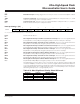
RID.7–0
Bits 7–0
Revision ID. The revision ID is a read-only value that reflects the current revision ID of the
device.This value is permanently set at manufacturing time and cannot be changed. The RID is
composed of two nibbles representing an alpha and a numeric character. For example, the RID of
the A2 revision contains 10100010b, and the B1 revision contains 10110001b. Any A revision
device of the DS89C420 contains the value FFh.
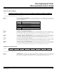
PAGEE
Bits 7
PAGES1, PAGES0
Bits 6, 5
Page Mode Enable. When set (= 1), page mode access is enabled for external bus operations as
configured by the page mode select bits PAGES1, PAGES0. When clear (= 0), external bus oper-
ations default to the standard 8051 expanded bus configuration.
Page Mode Select. If PAGEE = 1, these bits select the page mode configuration that is followed
for external bus operations. The four possible configurations are summarized in the table below.
Mode 1 results in Port 0 serving as the data bus and Port 2 being the multiplexed address
MSB/LSB. Mode 2 results in Port 0 being used strictly for address LSB and Por
t 2 being multiplexed
between address MSB and data.
Bits 4–0 Reserved. Read data is 1.
R = Unrestricted read, W = Unrestricted write, T = Timed-access write only, -n = Value after reset
Address Control (ACON)
R = Unrestricted read, W = Unrestricted write, -n = Value after reset, * = see description
Revision ID (RID)
76543210
SFR 9Ah RID.7 RID.6 RID.5 RID.4 RID.3 RID.2 RID.1 RID.0
R-* R-* R-* R-* R-* R-* R-* R-*
76 543 2 10
SFR 9Dh PAGEE PAGES1 PAGES0 — — — — —
RT-0 RT-0 RT-0 R-1 R-1 R-1 R-1 R-1
Table 4-11. Memory Access Cycle
PAGES 1-0
MODE PAGE-HIT PAGE-MISS
00 1 1 2
01 1 2 4
10 1 4 8
11 2 2 4
R = Unrestricted read, W = Unrestricted write, -n = Value after reset
Serial Data Buffer 0 (SBUF0)
7 6543210
SFR 99h SBUF0.7 SBUF0.6 SBUF0.5 SBUF0.4 SBUF0.3 SBUF0.2 SBUF0.1 SBUF0.0
RW-0 RW-0 RW-0 RW-0 RW-0 RW-0 RW-0 RW-0
Ultra-High-Speed Flash
Microcontroller User’s Guide
Maxim Integrated