
Owner's manual


4-18
Ultra-High-Speed Flash
Microcontroller User’s Guide
R = Unrestricted read, W = Unrestricted write, -n = Value after reset
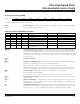
Clock Control (CKCON)
76543210
SFR 8Eh WD1 WD0 T2M T1M T0M MD2 MD1 MD0
RW-0 RW-0 RW-0 RW-0 RW-0 RW-0 RW-0 RW-1
TL1.7–0
Bits 7–0
Timer 1 LSB. This register contains the least significant byte of Timer 1.
TH0.7–0
Bits 7–0
Timer 0 MSB. This register contains the most significant byte of Timer 0.
TH1.7–0
Bits 7–0
Timer 1 MSB. This register contains the most significant byte of Timer 1.
WD1, WD0
Bits 7, 6
Watchdog Timer Mode Select 1-0. These bits determine the watchdog timer timeout period for
the watchdog timer. The timer divides the crystal (or external oscillator) frequency by a program-
mable value as shown on the next page. The divider value is expressed in crystal (oscillator)
cycles. The settings of the system clock control bits 4X/2X (PMR.3) and CD1:0 (PMR.7-6) affect the
clock input to the watchdog timer and therefore its timeout period as shown below. All watchdog
timer reset timeouts follow the setting of the interrupt flag by 512 system clocks.
Table 4-7. Watchdog Interrupt Flag Timeout Periods (in Oscillator Clocks)
4X/2X C D1:0 WD1 :0 = 00 WD1 :0 = 01 WD1 :0 = 10 W D1 :0 = 11
1 00 2
15
2
18
2
21
2
24
0 00 2
16
2
19
2
22
2
25
X 01 2
17
2
20
2
23
2
26
X 10 2
17
2
20
2
23
2
26
X 11 2
27
2
30
2
33
2
36
R = Unrestricted read, W = Unrestricted write, -n = Value after reset
Timer 1 MSB (TH1)
7 6 5 4 3 2 1 0
SFR 8Dh TH1.7 TH1.6 TH1.5 TH1.4 TH1.3 TH1.2 TH1.1 TH1.0
RW-0 RW-0 RW-0 RW-0 RW-0 RW-0 RW-0 RW-0
R = Unrestricted read, W = Unrestricted write, -n = Value after reset
Timer 0 MSB (TH0)
7 6 5 4 3 2 1 0
SFR 8Ch TH0.7 TH0.6 TH0.5 TH0.4 TH0.3 TH0.2 TH0.1 TH0.0
RW-0 RW-0 RW-0 RW-0 RW-0 RW-0 RW-0 RW-0
R = Unrestricted read, W = Unrestricted write, -n = Value after reset
Timer 1 LSB (TL1)
7 6 5 4 3 2 1 0
SFR 8Bh TL1.7 TL1.6 TL1.5 TL1.4 TL1.3 TL1.2 TL1.1 TL1.0
RW-0 RW-0 RW-0 RW-0 RW-0 RW-0 RW-0 RW-0
Maxim Integrated