
Owner's manual


4-13
SP.7–0
Bits 7–0
Stack Pointer. This stack pointer is written by software to identify the location where the stack
begins. The stack pointer is incremented before every PUSH operation and is decremented fol-
lowing every POP operation. This register defaults to 07h after reset.
P0.7–0
Bits 7–0
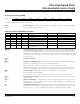
Port 0. This port functions according to the table below where PAGEE = ACON.7 and PAGES =
ACON.6-5.
When serving as general-purpose I/O (GPIO), the por
t is open-drain and requires pullups. Writing
a 1 to one of the bits of this register configures the associated port 0 pin as an input. All read oper-
ations, with the exception of read-modify-write instructions, leave the port latch unchanged. During
external memory addressing and data memory write cycles, the port has high-and-low drive capa-
bility. During external memory data read cycles, the port is held in a high-impedance state.
DPL.7–0
Bits 7–0
Data Pointer LOW 0. This register is the low byte of the standard 80C32 16-bit data pointer. DPL
and DPH are used to point to nonscratchpad data RAM.
R = Unrestricted read, W = Unrestricted write, -n = Value after reset
Data Pointer Low 0 (DPL)
76543210
SFR 82h DPL.7 DPL.6 DPL.5 DPL.4 DPL.3 DPL.2 DPL.1 DPL.0
RW-0 RW-0 RW-0 RW-0 RW-0 RW-0 RW-0 RW-0
Stack Pointer (SP)
76543210
SFR 81h SP.7 SP.6 SP.5 SP.4 SP.3 SP.2 SP.1 SP.0
RW-0 RW-0 RW-0 RW-0 RW-0 RW-1 RW-1 RW-1
R = Unrestricted read, W = Unrestricted write, -n = Value after reset
Port 0 (P0)
76543210
SFR 80h P0.7 P0.6 P0.5 P0.4 P0.3 P0.2 P0.1 P0.0
RW-1 RW-1 RW-1 RW-1 RW-1 RW-1 RW-1 RW-1
R = Unrestricted read, W = Unrestricted write, -n = Value after reset
Special-Function Registers
Most of the unique features of the ultra-high-speed microcontroller family are controlled by bits in SFRs located in unused loca-
tions in the 8051 SFR map. This allows for increased functionality while maintaining complete instruction set compatibility.
The description for each bit indicates its read and write access, as well as its state after a power-on reset.
PAGEE PAGES PORT 0 FUNCTION
0 XX General-Purpose I/O (code execution < ROMSIZE.2-0)
0 XX Multiplexed Address LSB / Data (code execution > ROMSIZE.2-0)
1 00, 01, 10 Data
1 11 Address LSB
Table 4-4. Port 0 Function
Ultra-High-Speed Flash
Microcontroller User’s Guide
Maxim Integrated