
Owner's manual


12-4
Ultra-High-Speed Flash
Microcontroller User’s Guide
When not using the power-management mode, the baud rate for mode 2 is a function only of the oscillator frequency. It is either the
oscillator input divided by 32 or 64 as programmed by the SMOD doubler bit for the associated UART. The SMOD_0 baud-rate dou-
bler bit for serial port 0 is located at PCON.7, and the SMOD_1 baud-rate doubler bit for serial port 1 is located at WDCON.7. Mode 2
operation is identical to the standard 80C32.
Mode 3
This mode has the same functionality as mode 2, but generates baud rates like mode 1. That is, this mode transmits 11 bits, but gen-
erates baud rates through the timers. Like mode 1, either timer 1 or 2 can be used for serial port 0 and timer 1 can be used for serial
port 1. Mode 3 operation is identical to the standard 80C32 when timers 1 or 2 use the default oscillator divide-by-12 as an input clock.
Serial Port Initialization
In order to use the UART function(s), the serial port must be initialized. This involves selecting the mode and time base, then initializing the
baud-rate generator, if necessary. Serial communication is then available. Once the baud-rate generator is running, the UART can receive data.
In mode 0, the high-speed microcontroller provides the clock. Serial reception is initiated by setting the RI bit to a logic 0 and REN to
a logic 1. This generates a clock on the TXD pin and a shift in the 8 bits on the RXD pin. In the other modes, setting the REN bit to a
logic 1 allows serial reception, but the external device must actually initiate it by sending a start bit. In any mode, serial transmission
is initiated by writing to either the SBUF0 or SBUF1 location.
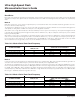
Most of the serial port controls are provided by the SCON0 and SCON1 registers. For convenience, the Table 12-2 is provided, which
summarizes the SFRs controlling serial port operation. Detailed bit descriptions can be found in Section 4.
Table 12-2. SFR Serial Port Operation Control
BIT N AMES DESCRIPTION REGISTER LOCA TION BIT POSITIONS
SM0/FE_0 Ser ial mode select 0 or framing error S CO N0 – 98h SCON 0.7
SM1_0 Ser ial mode select 1 S CON 0 – 98h SCON0.6
SM2_0 Ser ial mode select 2 S CON 0 – 98h SCON0.5
REN_0 Receive enable SCO N0 – 98h SCON 0.4
TB8_0 9thtransmit data bit SCO N0 – 98h SCON 0.3
RB8_0 9th receive data bit SCON0 – 98h SCO N0.2
TI_0 Transmit interrupt flag SCO N0 – 98h SCON 0.1
RI_0 Receive interrupt flag SCO N0 – 98h SCON 0.0
SMO D_ 0 Baud-rate doubler bit PCO N – 87h P CON.7
RCLK Timer 2 serial receive clock enable T2CON – C8h T2CON.5
TCLK Timer 2 ser ial trans mit clock enable T2CON – C8h T2CON.4
Serial data buffer SBUF0 – 99h
Slave address SADD R0 – A9h
SERIAL PO RT 0
Slave address mask enable SADEN0 – B9h
SM0/FE_1 Ser ial mode select 0 or framing error SC ON1 – C0h SCON1.7
SM1_1 Ser ial mode select 1 SCO N1 – C0h SCON1.6
SM2_1 Ser ial mode select 2 SCO N1 – C0h SCON1.5
REN_1 Receive enable SCO N1 – C0h SCON1.4
TB8_1 9thtransmit data bit SC ON1 – C0h SCON1.3
RB8_1 9th receive data bit SCO N1 – C0h SCON1.2
TI_1 Transmit interrupt flag SC ON1 – C0h SCON1.1
RI_1 Receive inter rupt flag SCO N1 – C0h SCON1.0
SMO D_ 1 Baud-rate doubler bit WD CON – D 8h WDCO N.7
Serial data buffer SBUF1 – C1h
Slave address SAD DR1 – AAh
SERIAL PO RT 1
Slave address mask enable SADEN1 – BAh
SMO D0 Enable framing er ror detection PCO N – 87h P CON.6
Maxim Integrated