
Owner's manual


7-10
Ultra-High-Speed Flash
Microcontroller User’s Guide
INTERNAL
SYSTEM
CLOCK
(
PMM
)
MINIMUM INSTRUCTION CYCLE
EXTERNAL
CLOCK
1024 CLOCKS
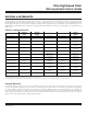
Figure 7-3. Internal Timing Relationships in PMM
PMM and Peripheral Functions
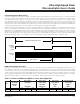
Timers 0, 1, and 2 default on reset to a 12 clock per cycle operation to remain compatible with the original 8051 timing. The timers can
be individually configured to run at the fastest instruction cycle timing (divide-by-1) or to a system clock divide-by-4 input by setting
the relevant bits in the clock control register (CKCON;8Eh). Because the timers derive their time base from the internal clock, timers 0,
1, and 2 operate at reduced clock rates during PMM. This also affects the operation of the serial ports in PMM. In general, it is not pos-
sible to generate standard baud rates while in PMM, and the user is advised to avoid PMM, or use the switchback feature, if serial port
operation is desired. Table 7-4 shows the effect of the PMM clock divider option on timer and serial port operation.
Table 7-4. Effect of PMM Clock Mode on Timer, Serial Operation
C D1:0
OSC
CYC LES PER
MA C H IN E
CYC LE
OSC CYCLES
PER TIMER
0/1/2 CLOC K
TxMH , TxM =
OSC CYCLES
PE
R TIMER 2
C LOC K, BA U D -
R
A TE GEN.
TxMH , TxM =
OSC C
YCLES
PER SERIAL
PORT C LOC K
MOD
E 0
SM2 =
OSC CYCLES PER
SERIAL
PORT C LOC K
MOD E 2
SMOD =
00 01 1x xx 010 1
11 1024 3072 1024 1024 2048 3072 1024 16,348 8192
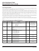
Power Management Mode Timing
The power management mode reduces power consumption by internally dividing the clock signal to the device, causing it to operate
at a reduced speed. When PMM is invoked, the external crystal continues to operate at full speed. The difference is that the device
uses 1024 external clocks to generate each system clock cycle as opposed to one clock per internal system clock cycle in the default
state. Relative timing relationships of all signals when the device is operating in PMM remains the same as the one cycle timing. Note
that all internal functions, on-board timers (including serial port baud-rate generation), watchdog timer, and software timing loops also
run at the reduced speed. Most applications do not find it necessary to attend to this much detail, but the information is provided for
calculating critical timings. Figure 7-2 demonstrates the internal timing relationships during PMM.
PMM is entered and exited by setting the clock rate divider bits (PMR.7-6). In addition, it is possible use the switchback feature to effect
a return to the divide-by-1 mode from the power management mode. This allows both hardware and software to cause an exit from
PMM. Entry to or exit from PMM must be done through the divide-by-1 mode (CD1:0 = 10b). This means that to switch from divide-by-
1024 to the crystal multiplier 4X mode or vice versa, one must first switch back to divide-by-1 mode. Attempts to execute an illegal
speed change are ignored, and the bits remain unchanged. It is the responsibility of the software to test for serial port activity before
attempting to change speed, as a modification of the clock divider bits during a serial port operation corrupts the data.
Maxim Integrated