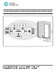
ULTRA-HIGH-SPEED FLASH MICROCONTROLLER USER’S GUIDE 33 FLASH MEMORY SRAM MIPS 25 8051 MICROPROCESSOR 5 DECREMENT 1 PORTS 0 ORIGINAL 8051 ULTRA-HIGH-S PEED FLASH MICROCONTRO LLER Functional Diagrams The Ultra-High-Speed Flash Microcontroller User’s Guide should be used in conjunction with the data sheet(s) for all ultra-high-speed flash microcontrollers. Pin Configurations appear at end of data sheet. Functional Diagrams continued at end of data sheet.
Ultra-High-Speed Flash Microcontroller User’s Guide REVISION HISTORY REVISION NUMBER REVISION DATE SECTION NUMBER PAGES CHANGED 0 1/01 — Initial release. 1 10/02 — Corrected some typos. 2 12/02 — Changed title to reflect “flash” and removed “DS89C420” reference. All 3 8/03 — Made document universal to all Dallas ultra-high-speed microcontrollers. All 4 Clarified that the CTM bit is cleared in stop mode. 14 5 Corrected cycle times for ADDC A, Rn instruction.
Ultra-High-Speed Flash Microcontroller User’s Guide SECTION 1: INTRODUCTION Maxim’s ultra-high-speed flash microcontroller is an 8051-compatible microcontroller that provides improved performance and power consumption when compared to the original 8051 version. It retains instruction set and object code compatibility with the 8051, yet performs the same operations in fewer clock cycles. Consequently, greater throughput is possible for the same crystal speed.
Ultra-High-Speed Flash Microcontroller User’s Guide SECTION 2: ORDERING INFORMATION The ultra-high-speed flash microcontroller family follows the part numbering convention shown below. Note that not all combinations of devices may be currently available. Contact a Maxim sales office for up-to-date details.
Ultra-High-Speed Flash Microcontroller User’s Guide SECTION 3: ARCHITECTURE This section contains the following information: ALU . . . . . . . . . . . . . . . . . . . . . . . . . . . . . . . . . . . . . . . . . . . . . . . . . . . . . . . . . . . . . . . . . . . . . . . . .3-2 Special-Function Registers . . . . . . . . . . . . . . . . . . . . . . . . . . . . . . . . . . . . . . . . . . . . . . . . . . . . . . .3-2 Accumulator . . . . . . . . . . . . . . . . . . . . . . . . . . . . . . . . . . . . . . . . .
Ultra-High-Speed Flash Microcontroller User’s Guide SECTION 3: ARCHITECTURE The architecture is based on the industry-standard 87C52 and executes the standard 8051 instruction set. The core is an accumulator-based architecture using internal registers for data storage and peripheral control. This section provides a brief description of each architecture feature. Details concerning the programming model, instruction set, and register description are provided in Section 4.
Ultra-High-Speed Flash Microcontroller User’s Guide Scratchpad Registers (RAM) The high-speed core provides 256 bytes of scratchpad RAM for general-purpose data and variable storage. The first 128 bytes are directly available to software. The second 128 are available through indirect addressing. Selected portions of this RAM have other optional functions. Stack The stack is a RAM area that stores return address information during calls and interrupts.
Ultra-High-Speed Flash Microcontroller User’s Guide Flash Memory On-chip program memory is implemented in flash memory. This can be programmed in-system with the standard 5V VCC supply through a serial port (in-system) using a built-in program memory loader, or by a standard flash or EPROM programmer. Full programming details are given in Section 15. A memory management unit (MMU) and other hardware supports any of the three programming methods.
Ultra-High-Speed Flash Microcontroller User’s Guide SECTION 4: PROGRAMMING MODEL This section contains the following information: Memory Organization . . . . . . . . . . . . . . . . . . . . . . . . . . . . . . . . . . . . . . . . . . . . . . . . . . . . . . . . . . .4-5 Memory Map . . . . . . . . . . . . . . . . . . . . . . . . . . . . . . . . . . . . . . . . . . . . . . . . . . . . . . . . . . . . . . . . .4-5 Register Map . . . . . . . . . . . . . . . . . . . . . . . . . . . . . . . . . . . . . . . . . .
Ultra-High-Speed Flash Microcontroller User’s Guide Timer Mode Control (TMOD) . . . . . . . . . . . . . . . . . . . . . . . . . . . . . . . . . . . . . . . . . . . . . . . . .4-17 Timer 0 LSB (TL0) . . . . . . . . . . . . . . . . . . . . . . . . . . . . . . . . . . . . . . . . . . . . . . . . . . . . . . . . .4-17 Timer 1 LSB (TL1) . . . . . . . . . . . . . . . . . . . . . . . . . . . . . . . . . . . . . . . . . . . . . . . . . . . . . . . . .4-18 Timer 0 MSB (TH0) . . . . . . . . . . . . . . . . . . . . .
Ultra-High-Speed Flash Microcontroller User’s Guide Timer 2 Capture LSB (RCAP2H) . . . . . . . . . . . . . . . . . . . . . . . . . . . . . . . . . . . . . . . . . . . . . .4-34 Timer 2 LSB (TL2) . . . . . . . . . . . . . . . . . . . . . . . . . . . . . . . . . . . . . . . . . . . . . . . . . . . . . . . . .4-35 Timer 2 MSB (TH2) . . . . . . . . . . . . . . . . . . . . . . . . . . . . . . . . . . . . . . . . . . . . . . . . . . . . . . . . .4-35 Program Status Word (PSW) . . . . . . . . . . . . . . . . . . .
Ultra-High-Speed Flash Microcontroller User’s Guide LIST OF TABLES Table 4-1. Instructions that Affect Flag Settings . . . . . . . . . . . . . . . . . . . . . . . . . . . . . . . . . . . . . .4-10 Table 4-2. Special-Function Register Locations . . . . . . . . . . . . . . . . . . . . . . . . . . . . . . . . . . . . . .4-11 Table 4-3. Special-Function Register Reset Values . . . . . . . . . . . . . . . . . . . . . . . . . . . . . . . . . . . .4-12 Table 4-4. Port 0 Function . . . . . . . . . . . . . . . . . .
Ultra-High-Speed Flash Microcontroller User’s Guide SECTION 4: PROGRAMMING MODEL This section provides a programmer’s overview of the ultra-high-speed microcontroller core. It includes information on the memory map, on-chip RAM, SFRs, and instruction set. The programming model of the ultra-high-speed microcontroller is very similar to that of the industry-standard 80C52. The memory map is identical. It uses the same instruction set, with improved instruction timing. Several new SFRs have been added.
Ultra-High-Speed Flash Microcontroller User’s Guide FFFFh 64k PROGRAM MEMORY FFh DATA MEMORY 255 INDIRECT RAM 7Fh 128 DIRECT SPECIAL FUNCTION REGISTERS FFh 7Fh DIRECT RAM 0000h 0000h Figure 4-2. Register Map Figure 4-1.
Ultra-High-Speed Flash Microcontroller User’s Guide Bit Addressable Locations In addition to direct register access, some individual bits are also accessible. These are individually addressable bits in both the RAM and SFR area. In the scratchpad RAM area, registers 20h to 2Fh are bit addressable. This provides 128 (16 x 8) individual bits available to software. A bit access is distinguished from a full register access by the type of instruction. Addressing modes are discussed later in this section.
Ultra-High-Speed Flash Microcontroller User’s Guide Register Addressing Register addressing is used for operands that are located in one of the eight working registers (R7–R0). The eight working registers can be located in one of four working register banks found in the lower 32 bytes of scratchpad RAM, as determined by the current register bank-select bits. A register bank is selected using two bits in the program status word (PSW;D0h).
Ultra-High-Speed Flash Microcontroller User’s Guide The 16-bit data pointers (DPTRs) can be used as an absolute off-chip reference. This gives access to the entire 64kB data memory map. An example is as follows: MOVX @DPTR, A ;Write the value in the accumulator ;to the address referenced by the ;selected data pointer. Immediate Addressing Immediate addressing is used when one of the operands is predetermined and coded into the software.
Ultra-High-Speed Flash Microcontroller User’s Guide Program Status Flags All program status flags are contained in the program status word at SFR location D0h. It contains flags that reflect the status of the CPU and the result of selected operations. The flags are summarized below. The following table shows the instructions that affect each flag. Bit Description*: PSW.7 C Carry Set when the previous operation resulted in a carry (during addition) or a borrow (during subtraction). Otherwise cleared.
Ultra-High-Speed Flash Microcontroller User’s Guide Table 4-2.
Ultra-High-Speed Flash Microcontroller User’s Guide Table 4-3.
Ultra-High-Speed Flash Microcontroller User’s Guide Special-Function Registers Most of the unique features of the ultra-high-speed microcontroller family are controlled by bits in SFRs located in unused locations in the 8051 SFR map. This allows for increased functionality while maintaining complete instruction set compatibility. The description for each bit indicates its read and write access, as well as its state after a power-on reset. Port 0 (P0) SFR 80h 7 P0.7 RW-1 6 P0.6 RW-1 5 P0.5 RW-1 4 P0.
Ultra-High-Speed Flash Microcontroller User’s Guide Data Pointer High 0 (DPH) SFR 83h 7 DPH.7 RW-0 6 DPH.6 RW-0 5 DPH.5 RW-0 4 DPH.4 RW-0 3 DPH.3 RW-0 2 DPH.2 RW-0 1 DPH.1 RW-0 0 DPH.0 RW-0 R = Unrestricted read, W = Unrestricted write, -n = Value after reset DPH.7–0 Bits 7–0 Data Pointer High 0. This register is the high byte of the standard 80C32 16-bit data pointer. DPL and DPH are used to point to nonscratchpad data RAM. Data Pointer Low 1 (DPL1) SFR 84h 7 DPL1.7 RW-0 6 DPL1.
Ultra-High-Speed Flash Microcontroller User’s Guide TSL Bit 5 Toggle Select. When clear (= 0), DPTR-related instructions do not affect the SEL bit. When set (= 1), the SEL bit is toggled following execution of any of the below DPTR-related instructions: INC DPTR MOV DPTR, #data16 MOVC A, @A+DPTR MOVX A, @DPTR MOVX @DPTR, A Autoincrement/Decrement Enable.
Ultra-High-Speed Flash Microcontroller User’s Guide STOP Bit 1 Stop Mode Select. Setting this bit stops program execution, halts the CPU oscillator and internal timers, and places the CPU in a low-power mode. This bit always be reads as a 0. Setting this bit causes the CTM bit (PMR.4) to be cleared. Setting both the STOP bit and the IDLE bit causes the device to enter stop mode; however, doing this is not advised. IDLE Bit 0 Idle Mode Select.
Ultra-High-Speed Flash Microcontroller User’s Guide Timer Mode Control (TMOD) SFR 89h 7 GATE RW-0 6 C/T RW-0 5 M1 RW-0 4 M0 RW-0 3 GATE RW-0 2 C/T RW-0 1 M1 RW-0 0 M0 RW-0 R = Unrestricted read, W = Unrestricted write, -n = Value after reset GATE Bit 7 Timer 1 Gate Control. This bit enables/disables the ability of Timer 1 to increment. C/T Bit 6 Timer 1 Counter/Timer Select. 0 = Timer 1 clocks when TR1 = 1, regardless of the state of INT. 1 = Timer 1 clocks only when TR1 = 1 and INT1 = 1.
Ultra-High-Speed Flash Microcontroller User’s Guide Timer 1 LSB (TL1) SFR 8Bh 7 TL1.7 RW-0 6 TL1.6 RW-0 5 TL1.5 RW-0 4 TL1.4 RW-0 3 TL1.3 RW-0 2 TL1.2 RW-0 1 TL1.1 RW-0 0 TL1.0 RW-0 R = Unrestricted read, W = Unrestricted write, -n = Value after reset TL1.7–0 Bits 7–0 Timer 1 LSB. This register contains the least significant byte of Timer 1. Timer 0 MSB (TH0) SFR 8Ch 7 TH0.7 RW-0 6 TH0.6 RW-0 5 TH0.5 RW-0 4 TH0.4 RW-0 3 TH0.3 RW-0 2 TH0.2 RW-0 1 TH0.1 RW-0 0 TH0.
Ultra-High-Speed Flash Microcontroller User’s Guide T2M Bit 5 Timer 2 Clock Select. This bit controls the input clock that drives Timer 2. This bit has no effect when the timer is in baud rate generator or clock output modes. See Timer Operation table. T1M Bit 4 Timer 1 Clock Select. This bit controls the input clock that drives Timer 1. See Timer Operation table. T0M Bit 3 Timer 0 Clock Select. This bit controls the input clock that drives Timer 0. See Timer Operation table. Table 4-8.
Ultra-High-Speed Flash Microcontroller User’s Guide Port 1 (P1) SFR 90h 7 6 5 4 3 2 1 0 P1.7 INT5 P1.6 INT4 P1.5 INT3 P1.4 INT2 P1.3 TXD1 P1.2 RXD1 P1.1 T2EX P1.0 T2 RW-1 RW-1 RW-1 RW-1 RW-1 RW-1 RW-1 RW-1 R = Unrestricted read, W = Unrestricted write, -n = Value after reset P1.7–0 Bits 7–0 General-Purpose I/O Port 1. This register functions as a general-purpose I/O port. In addition, all the pins have an alternative function listed below.
Ultra-High-Speed Flash Microcontroller User’s Guide CKRY Bit 3 Clock Ready. This bit indicates the status of the startup period for the crystal oscillator or crystal multiplier warm-up period. This bit is cleared after a reset or when exiting STOP mode. It is also cleared when the clock multiplier is enabled (setting of PMR.4 = 1). Once CKRY is cleared, a 65,536 clock count must take place before CKRY is set and the lockout preventing modification of CD1:CD0 is removed.
Ultra-High-Speed Flash Microcontroller User’s Guide Serial Port 0 Control (SCON0) 7 SM0/FE_0 RW-0 SFR 98h 6 SM1_0 RW-0 5 SM2_0 RW-0 4 REN_0 RW-0 3 TB8_0 RW-0 2 RB8_0 RW-0 1 TI_0 RW-0 0 RI_0 RW-0 R = Unrestricted read, W = Unrestricted write, -n = Value after reset SM0–2 Bits 7, 6, 5 Serial Port Mode. These bits control the mode of serial port 0. In addition the SM0 and SM2_0 bits have secondary functions as shown. Table 4-10.
Ultra-High-Speed Flash Microcontroller User’s Guide RI_0 Bit 0 Receiver Interrupt Flag. This bit indicates that a byte of data has been received in the serial port 0 buffer. In serial port mode 0, RI_0 is set at the end of the 8th bit. In serial port mode 1, RI_0 is set after the last sample of the incoming stop bit subject to the state of SM2_0. In modes 2 and 3, RI_0 is set after the last sample of RB8_0. This bit must be manually cleared by software. Serial Data Buffer 0 (SBUF0) SFR 99h 7 SBUF0.
Ultra-High-Speed Flash Microcontroller User’s Guide Port 2 (P2) SFR A0h 7 P2.7 RW-1 6 P2.6 RW-1 5 P2.5 RW-1 4 P2.4 RW-1 3 P2.3 RW-1 2 P2.2 RW-1 1 P2.1 RW-1 0 P2.0 RW-1 R = Unrestricted read, W = Unrestricted write, -n = Value after reset P2.7–0 Bits 7–0 Port 2. This port functions according to the table below where PAGEE = ACON.7 and PAGES = ACON.6-5. Table 4-12. Port 2 Functions PAGEE 0 0 1 1 PAGES XX XX 00, 01, 10 11 PORT2 FUNCTION General-Purpose I/0 (code execution < ROMSIZE.
Ultra-High-Speed Flash Microcontroller User’s Guide ET0 Bit 1 Enable Timer 0 Interrupt. This bit controls the masking of the Timer 0 interrupt. 0 = Disable all Timer 0 interrupts. 1 = Enable all interrupt requests generated by the TF0 flag (TCON.5). EX0 Bit 0 Enable External Interrupt 0. This bit controls the masking of external interrupt 0. 0 = Disable external interrupt 0. 1 = Enable all interrupt requests generated by the INT0 pin. Slave Address Register 0 (SADDR0) SFR A9h 7 SADDR0.7 RW-0 6 SADDR0.
Ultra-High-Speed Flash Microcontroller User’s Guide INT0 Bit 2 External Interrupt 0. A falling edge/low level on this pin causes an external interrupt 0 if enabled. TXD0 Bit 1 RXD0 Bit 0 Serial Port 0 Transmit. This pin transmits the serial port 0 data in serial port modes 1, 2, 3 and emits the synchronizing clock in serial port mode 0. Serial Port 0 Receive. This pin receives the serial port 0 data in serial port modes 1, 2, 3 and is a bidirectional data transfer pin in serial port mode 0.
Ultra-High-Speed Flash Microcontroller User’s Guide Interrupt Priority 0 (IP0) SFR B8h 7 6 5 4 3 2 1 0 — LPS1 LPT2 LPS0 LPT1 LPX1 LPT0 LPX0 R-1 RW-0 RW-0 RW-0 RW-0 RW-0 RW-0 RW-0 R = Unrestricted read, W = Unrestricted write, -n = Value after reset IP07.0 Bit 7 Reserved. Read data is 1. LPS1 Bit 6 Least Significant Priority Select Bit for Serial Port 1 Interrupt. LPS1 is the least significant bit of the bit pair MPS1 (IP1.
Ultra-High-Speed Flash Microcontroller User’s Guide Slave Address Mask Enable Register 1 (SADEN1) SFR BAh 7 SADEN1.7 RW-0 6 SADEN1.6 RW-0 5 SADEN1.5 RW-0 4 SADEN1.4 RW-0 3 SADEN1.3 RW-0 2 SADEN1.2 RW-0 1 SADEN1.1 RW-0 0 SADEN1.0 RW-0 R = Unrestricted read, W = Unrestricted write, -n = Value after reset SADEN1.7–0 Bits 7–0 Slave Address Mask Enable Register 1. This register functions as a mask when comparing serial port 1 addresses for automatic address recognition.
Ultra-High-Speed Flash Microcontroller User’s Guide SM2_1 Bit 5 Multiple CPU Communications. The function of this bit is dependent on the serial port 1 mode. Mode 0: Selects period for synchronous port 1 data transfers. Mode 1: When this bit is set, reception is ignored (RI_1 is not set) if invalid stop bit received. Modes 2/3: When this bit is set, multiprocessor communications are enabled in mode 2 and 3.
Ultra-High-Speed Flash Microcontroller User’s Guide RMS2–0 Bits 2–0 ROM Memory Size Select 2-0. This register is used to select the maximum on-chip decoded address. Care must be taken that the memory location of the current program counter is valid both before and after modification. These bits can only be modified using a timed-access procedure. The EA pin overrides the function of these bits when asserted, forcing the device to access external program memory only.
Ultra-High-Speed Flash Microcontroller User’s Guide Table 4-17. Serial Port Operation (in Oscillator Clocks) 4X/2X CD1:0 1 CLOCK (MODE 0) CLOCK (MODE 2) SM2 = 0 SM2 = 1 SMOD = 0 00 3 1 64 32 0 00 6 2 64 32 X 01 12 4 64 32 X 10 12 4 64 32 X 11 3072 1024 16384 8192 SMOD = 1 SWB Bit 5 Switchback Enable. This bit allows an enabled external interrupt or serial port activity to force the clock divide control bits to the divide-by-1 state (01b).
Ultra-High-Speed Flash Microcontroller User’s Guide Status Register (STATUS) SFR C5 7 PIS2 R-0 6 PIS1 R-0 5 PIS0 R-0 4 — R-1 3 SPTA1 R-0 2 SPRA1 R-0 1 SPTA0 R-0 0 SPRA0 R-0 R = Unrestricted read, W = Unrestricted write, -n = Value after reset PIS2-0 Bit 7, 6, 5 Priority Interrupt Status Bits 2-0. These bits indicate the level of interrupt that is currently being serviced. (Interrupt levels 0-3 are associated with interrupt sources using the MP,LP bits found in the IP1 and IP0 SFRS.
Ultra-High-Speed Flash Microcontroller User’s Guide Timer 2 Control (T2CON) SFR C8h 7 TF2 RW-0 6 EXF2 RW-0 5 RCLK RW-0 4 TCLK RW-0 3 EXEN2 RW-0 2 TR2 RW-0 1 C/T2 RW-0 0 CP/RL2 RW-0 R = Unrestricted read, W = Unrestricted write, -n = Value after reset TF2 Bit 7 Timer 2 Overflow Flag. This flag is set when Timer 2 overflows from FFFFh or the count equal to the capture register in down count mode. It must be cleared by software. TF2 is only set if RCLKand TCLK are both cleared to 0.
Ultra-High-Speed Flash Microcontroller User’s Guide Capture/Reload Select. This bit determines whether the capture or reload function is used for Timer 2. When set (= 1), Timer 2 captures occur when a falling edge is detected on T2EX(P1.1) if EXEN2 = 1. When clear (= 0), Timer 2 functions in an autoreload mode. An autoreload occurs following each overflow if RCLK or TCLK is set or if a falling edge is detected on T2EX if EXEN2 = 1.
Ultra-High-Speed Flash Microcontroller User’s Guide Timer 2 LSB (TL2) SFR CCh 7 TL2.7 RW-0 6 TL2.6 RW-0 5 TL2.5 RW-0 4 TL2.4 RW-0 3 TL2.3 RW-0 2 TL2.2 RW-0 1 TL2.1 RW-0 0 TL2.0 RW-0 R = Unrestricted read, W = Unrestricted write, -n = Value after reset TL2.7–0 Bits 7–0 Timer 2 LSB. This register contains the least significant byte of Timer 2. Timer 2 MSB (TH2) SFR CDh 7 TH2.7 RW-0 6 TH2.6 RW-0 5 TH2.5 RW-0 4 TH2.4 RW-0 3 TH2.3 RW-0 2 TH2.2 RW-0 1 TH2.1 RW-0 0 TH2.
Ultra-High-Speed Flash Microcontroller User’s Guide Watchdog Control (WDCON) SFR D8h 7 SMOD_1 RW-0 6 POR RT-* 5 EPFI RW-0 4 PFI RW-* 3 WDIF RT-0 2 WTRF RW-* 1 EWT RT-* 0 RWT RT-0 R = Unrestricted read, W = Unrestricted write, T = Timed-access write only, -n = Value after reset, * = see description SMOD_1 Bit 7 Serial Modification. This bit controls the doubling of the serial port 1 baud rate in modes 1, 2, and 3. 0 = Serial port 1 baud rate operates at normal speed.
Ultra-High-Speed Flash Microcontroller User’s Guide RWT Bit 0 Reset Watchdog Timer. Setting this bit resets the watchdog timer count. This bit must be set using a Timed Access procedure before the watchdog timer expires, or a watchdog timer reset and/or interrupt is generated if enabled. The timeout period is defined by the Watchdog Timer Mode Select bits (CKCON.7-6). This bit is always 0 when read. Accumulator (A or ACC) SFR E0h 7 ACC.7 RW-0 6 ACC.6 RW-0 5 ACC.5 RW-0 4 ACC.4 RW-0 3 ACC.
Ultra-High-Speed Flash Microcontroller User’s Guide B Register (B) SFR F0h 7 B.7 RW-0 6 B.6 RW-0 5 B.5 RW-0 4 B.4 RW-0 3 B.3 RW-0 2 B.2 RW-0 1 B.1 RW-0 0 B.0 RW-0 R = Unrestricted read, W = Unrestricted write, -n = Value after reset B.7–0 Bits 7–0 B Register. This register serves as a second accumulator for certain arithmetic operations.
Ultra-High-Speed Flash Microcontroller User’s Guide Extended Interrupt Priority 0 (EIP0) SFR F8h 7 — R-1 6 — R-1 5 — R-1 4 LPWDI RW-0 3 LPX5 RW-0 2 LPX4 RW-0 1 LPX3 RW-0 0 LPX2 RW-0 R = Unrestricted read, W = Unrestricted write, -n = Value after reset Bits 7–5 Reserved. Read data is 1. LPWDI Bit 4 Least significant priority select bit for watchdog interrupt. This is the least significant bit of the bit pair MPWDI (EIP1.4), LPWDI that designates priority level for the watchdog interrupt.
Ultra-High-Speed Flash Microcontroller User’s Guide SECTION 5: CPU TIMING This section contains the following information: Oscillator . . . . . . . . . . . . . . . . . . . . . . . . . . . . . . . . . . . . . . . . . . . . . . . . . . . . . . . . . . . . . . . . . . . . .5-3 XTAL1 . . . . . . . . . . . . . . . . . . . . . . . . . . . . . . . . . . . . . . . . . . . . . . . . . . . . . . . . . . . . . . . . . . . . . . .5-3 XTAL2 . . . . . . . . . . . . . . . . . . . . . . . . . . . . . . . . . . . . . . . .
Ultra-High-Speed Flash Microcontroller User’s Guide LIST OF FIGURES Figure 5-1. Crystal Connection . . . . . . . . . . . . . . . . . . . . . . . . . . . . . . . . . . . . . . . . . . . . . . . . . . . .5-3 Figure 5-2. Clock Source Input . . . . . . . . . . . . . . . . . . . . . . . . . . . . . . . . . . . . . . . . . . . . . . . . . . .5-3 Figure 5-3. System Clock Sources . . . . . . . . . . . . . . . . . . . . . . . . . . . . . . . . . . . . . . . . . . . . . . . . .5-4 Figure 5-4.
Ultra-High-Speed Flash Microcontroller User’s Guide SECTION 5: CPU TIMING The timing of the ultra-high-speed microcontroller is the area with the greatest departure from the original 8051 series. This section explains the timing and compares it to the original 8051. Oscillator The ultra-high-speed microcontroller provides an on-chip oscillator circuit that can be driven by an external crystal or by an off-chip TTL clock source.
Ultra-High-Speed Flash Microcontroller User’s Guide System Clock Divide Control The ultra-high-speed microcontroller provides the ability to speed up or slow down the system clock that is used internally by the CPU. The system clock divide ratio can be configured to 0.25 (4X multiply mode), 0.5 (2X multiply mode), 1 (default), or 1024 (power management mode) and is controlled by the CD1:0 bits (PMR.7, PMR.6).
Ultra-High-Speed Flash Microcontroller User’s Guide MUX 00 01, 10 11 SYSTEM CLOCK EXECUTION INTERNAL EXTERNAL NON PAGE PAGE MODE 1 (1-CYCLE) PAGE MODE 1 (2-CYCLE) PAGE MODE 1 (3-CYCLE) PAGE MODE 2 MEMORY CYCLE SYSCLK/1 SYSCLK/4 SYSCLK/1 SYSCLK/2 SYSCLK/4 SYSCLK/2 (PROG) SYSCLK/4 (DATA) MEMORY CYCLE Figure 5-4. Instruction Memory Cycle Determination Instruction Timing The ultra-high-speed microcontroller executes the industry standard 8051 instruction set.
Ultra-High-Speed Flash Microcontroller User’s Guide 2-Byte Instructions All 2-byte instructions require a minimum of two cycles, since fetching each byte requires a separate memory access. The first byte is the instruction op code that is decoded by the CPU. The second byte is normally an operand, or it can specify the location of the operand. For example, “ADD A, direct” is a 2-byte, two-cycle instruction where the second byte specifies the direct address location of the operand.
Ultra-High-Speed Flash Microcontroller User’s Guide Nonpage Mode External Timing The ultra-high-speed flash microcontroller defaults to a nonpage mode external memory interface. The nonpage mode bus structure requires four system clock cycles per memory cycle. In the nonpage mode, the ALE signal latches the address LSB on each program fetch. When the cycle count of an instruction exceeds the byte count, “dummy” fetches are performed each cycle until instruction execution is complete.
Ultra-High-Speed Flash Microcontroller User’s Guide Figure 5-7 illustrates an ACALL instruction (2 bytes, two cycles) with a destination address residing on a different 256-byte page. This is indicated only by the MSB address change on port 2. The memory cycle duration remains constant. Figure 5-8 shows execution of the RET instruction (1 byte, three cycles). Because the cycle count of the RET instruction exceeds the byte count, two stall cycles (“dummy” fetches) are inserted to allow execution to complete.
Ultra-High-Speed Flash Microcontroller User’s Guide Page Mode 1 External Timing—Pages 1:0 = 10b (Four Cycles) The page mode 1 external bus structure multiplexes port 2 to provide the address MSB and LSB. Data transactions occur exclusively on port 0. ALE is used to latch the address MSB only when needed, and PSEN serves as the enable for external program memory. Page mode 1 must be initiated by internal code memory.
Ultra-High-Speed Flash Microcontroller User’s Guide Page Mode 1 External Timing—Pages 1:0 = 10b (Four Cycles) (continued) Figure 5-11 shows execution of the INC direct instruction (2 byte, two or three cycles) for the cases where an extra memory cycle is not (INC DPL) and is (INC DPS) required. Figure 5-12 illustrates execution of the ACALL instruction whose destination address is on a different 256-byte page.
Ultra-High-Speed Flash Microcontroller User’s Guide Page Mode 1 External Timing—Pages 1:0 = 10b (Four Cycles) (continued) Figure 5-13 and Figure 5-14 demonstrate the execution of the RET (1-byte, three cycles) instruction. In Figure 5-13, the return address resides on the same 256-byte page as that of the executed RET instruction. Two stall cycles are inserted followed by a page-hit memory cycle. In Figure 5-14, the return address is on a different 256-byte page from where the RET instruction was executed.
Ultra-High-Speed Flash Microcontroller User’s Guide Page Mode 1 External Timing—Pages 1:0 = 01b (Two Cycles) The page mode 1 external bus structure multiplexes port 2 to provide the address MSB and LSB. Data transactions occur exclusively on port 0. ALE is used to latch the Address MSB only when needed, and PSEN serves as the enable for external program memory. To invoke two-cycle page mode 1 operation, the PAGES1:0 bits must be set to 01b, followed by the setting of the PAGEE bit.
Ultra-High-Speed Flash Microcontroller User’s Guide Page Mode 1 External Timing—Pages 1:0 = 00b (One Cycle) The page mode 1 external bus structure multiplexes port 2 to provide the address MSB and LSB. Data transactions occur exclusively on port 0. ALE is used to latch the address MSB only when needed, and PSEN serves as the enable for external program memory.
Ultra-High-Speed Flash Microcontroller User’s Guide Page Mode 1 External Timing—Pages 1:0 = 00b (One Cycle) (continued) Figure 5-19 illustrates the JBC bit, rel (3 bytes, four cycles) instruction for the case where the tested bit is clear and the jump is not taken. Note that one stall cycle must be inserted since the cycle count exceeds the byte count by one. The RET (1 byte, three cycles) instruction that follows requires insertion of two stall cycles.
Ultra-High-Speed Flash Microcontroller User’s Guide Page Mode 2 External Timing—Pages 1:0 = 11b The page mode 2 external bus structure multiplexes port 2 between address MSB and data. The address LSB is provided exclusively on port 0. ALE is used to latch the address MSB only when needed, and PSEN serves as the enable for external program memory. To invoke page mode 2 operation, the PAGES 1:0 bits must be set to 11b, followed by the setting of the PAGEE bit.
Ultra-High-Speed Flash Microcontroller User’s Guide Comparison to the 8051 The original 8051 needed 12 clocks per machine cycle and most instructions executed in either one or two machine cycles. Thus, except for the MUL and DIV instructions, the 8051 used either 12 or 24 clocks for each instruction. Furthermore, each machine cycle in the 8051 used two memory fetches. In many cases the second fetch was a dummy, and the extra clock cycles were wasted.
Ultra-High-Speed Flash Microcontroller User’s Guide Table 5-1. Instruction Timing Comparison (continued) HEX CODE UHSM CLOCK CYCLES UHSM TIME @ 25MHz 8051 CLOCK CYCLES 8051 TIME @ 25MHz UHSM vs. 8051 SPEED ADVANTAGE 15 2 80 ns 12 480 ns 6 DEC @Ri 16..17 2 80 ns 12 480 ns 6 MUL AB A4 9 360 ns 48 960 ns 5.33 DIV AB 84 10 400 ns 48 960 ns 4.80 INSTRUCTION DEC direct DA A D4 2 80 ns 12 480 ns 6 58..5F 1 40 ns 12 480 ns 12 55 2 80 ns 12 480 ns 6 56..
Ultra-High-Speed Flash Microcontroller User’s Guide Table 5-1. Instruction Timing Comparison (continued) HEX CODE UHSM CLOCK CYCLES UHSM TIME @ 25MHz 8051 CLOCK CYCLES 8051 TIME @ 25MHz UHSM vs. 8051 SPEED ADVANTAGE MOV Rn, direct A8..AF 2 80 ns 24 960 ns 12 MOV Rn, #data 78..7F 2 80 ns 12 480 ns 6 MOV direct, A F5 2 80 ns 12 480 ns 6 MOV direct, Rn 88..8F 2 80 ns 24 960 ns 12 85 3 120 ns 24 960 ns 8 86..
Ultra-High-Speed Flash Microcontroller User’s Guide Table 5-1. Instruction Timing Comparison (continued) UHSM CLOCK CYCLES UHSM TIME @ 25MHz 8051 CLOCK CYCLES 8051 TIME @ 25MHz UHSM vs.
Ultra-High-Speed Flash Microcontroller User’s Guide Table 5-2. Instruction Speed Summary INSTRUCTION CATEGORY Total instructions: 1 byte Total instructions: 2 byte Total instructions: 3 byte Average across all instructions OPCODE CATEGORY Total opcodes: 1 byte Total opcodes: 2 byte Total opcodes: 3 byte Average across all opcodes Maxim Integrated SPEED ADVANTAGE QUANTITY 4.0 4.8 5.3 6.0 8.0 12.0 24.0 4.0 6.0 8.0 12.0 4.8 6.0 8.0 8.
Ultra-High-Speed Flash Microcontroller User’s Guide SECTION 6: MEMORY ACCESS This section contains the following information: Internal Flash Memory . . . . . . . . . . . . . . . . . . . . . . . . . . . . . . . . . . . . . . . . . . . . . . . . . . . . . . . . . .6-3 ROMSize Feature . . . . . . . . . . . . . . . . . . . . . . . . . . . . . . . . . . . . . . . . . . . . . . . . . . . . . . . . . . . . . .6-3 Flash Security Block/Lock Bits . . . . . . . . . . . . . . . . . . . . . . . . . . . . . . . . . . .
Ultra-High-Speed Flash Microcontroller User’s Guide LIST OF FIGURES Figure Figure Figure Figure Figure Figure Figure Figure Figure Figure Figure Figure Figure Figure Figure Figure Figure Figure Figure Figure Figure Figure 6-1. Memory Map for the DS89C420/430 . . . . . . . . . . . . . . . . . . . . . . . . . . . . . . . . . . . . . .6-5 6-2. Program Memory Interconnect (Nonpage Mode) . . . . . . . . . . . . . . . . . . . . . . . . . . . .6-7 6-3.
Ultra-High-Speed Flash Microcontroller User’s Guide SECTION 6: MEMORY ACCESS The ultra-high-speed flash microcontroller supports the memory interface convention established for the industry standard 80C51, but also implements two new page mode memory interfaces needed to support ultra-high-speed external operation. These external page mode interfaces are described later in this section. Program and data memory areas can be implemented on-chip, off-chip, or as a combination.
Ultra-High-Speed Flash Microcontroller User’s Guide Modification of the ROMSIZE (C2h) special function register requires using the timed access procedure and must be followed by a two machine cycle delay, such as executing two NOP instructions, before jumping to the new address range. Interrupts must be disabled during this operation, because a call to an interrupt vector during the changing of the memory map can cause erratic results.
Ultra-High-Speed Flash Microcontroller User’s Guide Option Control Register Byte User-selectable options are present that must be set before beginning software execution. The option control register uses flash bits, rather than SFRs, and is individually erasable and programmable as a byte-wide register. Bit 3 of this register is defined as the watchdog POR default.
Ultra-High-Speed Flash Microcontroller User’s Guide Internal SRAM Memory The ultra-high-speed microcontroller incorporates an internal 1kB SRAM that is usable as data, program, or merged program/data memory. Upon a power-on reset, the internal 1kB memory is disabled and transparent to both program and data memory maps. When used for data, the memory is addressed through MOVX commands, and is in addition to the 256 bytes of scratchpad memory.
Ultra-High-Speed Flash Microcontroller User’s Guide PSEN ALE PORT 0 CK 74F373 LATCH LSB ADDRESS (8) DATA BUS (8) MSB ADDRESS (7) OE 64kB X 8 MEMORY CE DS89C4x0 PORT 2 Figure 6-2. Program Memory Interconnect (Nonpage Mode) Figure 6-3 shows the timing relationship for internal and external nonpage mode code fetches when CD1:0 = 10b. Note that an external program fetch takes four system clocks, and an internal program fetch requires only one system clock.
Ultra-High-Speed Flash Microcontroller User’s Guide Program Memory Interface—Page Modes Page mode retains the basic external circuitry requirements as the original 8051 external memory interface, but modifies the address/data roles of P0 and P2 in order to achieve the most efficient single-cycle external operation possible. The functions of ALE and PSEN are also altered to support page mode operation. Page mode is enabled by setting the PAGEE (ACON.7) bit to a logic 1.
Ultra-High-Speed Flash Microcontroller User’s Guide Page Mode 1 Bus Structure The page mode 1 external bus structure uses P2 as the primary address bus (multiplexing both the most significant byte and least significant byte of the address for each external memory cycle), and P0 is used as the primary data bus. This program memory interconnect scheme is depicted in Figure 6-4.
Ultra-High-Speed Flash Microcontroller User’s Guide Figure 6-5 shows external memory cycles for the page mode 1 bus structure. The first case illustrates a back-to-back MOVX execution sequence for one-cycle page mode (PAGES 1:0 = 00b). PSEN remains active during page-hit cycles, and page misses are forced during and after MOVX executions, independent of the most significant byte of the subsequent addresses. The second case illustrates a MOVX execution sequence for two-cycle page mode (PAGES 1:0 = 01b).
Ultra-High-Speed Flash Microcontroller User’s Guide Page Mode 2 Bus Structure The page mode 2 external bus structure multiplexes the most significant address byte with data on P2 and uses P0 for the least significant address byte. An illustration of this memory interface is provided in Figure 6-6. This bus structure speeds up external code fetches only.
Ultra-High-Speed Flash Microcontroller User’s Guide Data Memory Interface As described in Section 4, the ultra-high-speed microcontroller provides a small amount of RAM mapped as registers for on-chip direct access. This is not considered data memory and does not fall into the memory map. Systems that require more RAM or memorymapped peripherals must use the data memory area. This segment is a 64kB space located between 0000h and FFFFh. It is reached using the MOVX instruction.
Ultra-High-Speed Flash Microcontroller User’s Guide CK 74F373 LATCH ALE PORT 0 LSB ADDRESS (8) DATA BUS (8) MSB ADDRESS (8) 64kB X 8 SRAM CE DS89C4x0 PORT 2 RD (P3.7) OE WR (P3.6) WE Figure 6-8. Data Memory Interconnect (Nonpage Mode) External Data Memory Interface—Page Modes The ultra-high-speed flash microcontroller allows software to adjust the speed of external data memory access by stretching the memory bus cycle in page mode operation just like nonpage mode operation.
Ultra-High-Speed Flash Microcontroller User’s Guide Table 6-6. Page Mode 1—Data Memory Stretch Values Two Cycles (Pages 1:0 = 01b) RD/WR PULSE WIDTH (IN NUMBER OF OSCILLATOR CLOCKS) MD2:MD0 (STRETCH VALUE) STRETCH CYCLES 4X/2X, CD1, CD0 = 100 4X/2X, CD1, CD0 = 000 4X/2X, CD1, CD0 = X10 4X/2X, CD1, CD0 = X11 000 001 010 011 100 101 110 111 0 1 2 3 7 8 9 10 0.25 0.75 1.75 2.75 3.75 4.75 5.75 6.75 0.5 1.5 3.5 5.5 7.5 9.5 11.5 13.
Ultra-High-Speed Flash Microcontroller User’s Guide Figures 6-9 and 6-10 show data memory interconnect examples for page mode 1 and page mode 2. ALE PORT 2 CK 74F373 LATCH DS89C4x0 PORT 0 MSB ADDRESS (8) LSB ADDRESS (8) DATA BUS (8) RD (P3.7) 64kB X 8 SRAM CE OE WR (P3.6) WE Figure 6-9. Data Memory Interconnect (Page Mode 1) ALE PORT 2 DS89C4x0 PORT 0 RD (P3.7) WR (P3.6) CK 74F373 LATCH MSB ADDRESS (8) DATA BUS (8) LSB ADDRESS (8) 64kB X 8 SRAM CE OE WE Figure 6-10.
Ultra-High-Speed Flash Microcontroller User’s Guide Figures 6-11 to 6-22 illustrate the external data memory timing for the nonpage and page mode external bus structures. Nonpage Mode Data Memory Timing Figure 6-11 shows execution of the MOVX instruction from internal program memory with stretch value = 0 assigned (MD2:0 = 000b). Note that the internal memory cycles consist of one system clock while the external memory cycles always consist of four system clocks.
Ultra-High-Speed Flash Microcontroller User’s Guide Page Mode 1 Data Memory Timing–PAGES 1:0 = 10b (Four Cycles) Figure 6-13 shows execution of the MOVX instruction from internal program memory with stretch value = 0 assigned (MD2:0 = 000b). Note that the internal memory cycles consist of one system clock while the external memory cycles consist of four system clocks (page hit) or eight system clocks (page miss). Figure 6-14 illustrates the same MOVX instruction with a default stretch value (MD2:0 = 001b).
Ultra-High-Speed Flash Microcontroller User’s Guide Page Mode 1 Data Memory Timing–Pages 1:0 = 01b (Two Cycles) Figure 6-15 below shows execution of back-to-back MOVX instructions from internal flash memory. A stretch value = 0 (MD2:0 = 000b) has been assigned. Note that the internal memory cycles consist of one system clock while the external memory cycles consist of two system clocks (page hit) or four system clocks (page miss).
Ultra-High-Speed Flash Microcontroller User’s Guide Page Mode 1 Data Memory Timing–Pages 1:0 = 01b (Two Cycles) (continued) Figure 6-17 shows execution of a MOVX instruction with default stretch value = 1 (MD2:0 = 001b) from external program memory. The most probable case, where a page-miss is needed for the MOVX instruction, is given here. However, if the MOVX address happened to coincide with the current code execution page, a page hit would occur.
Ultra-High-Speed Flash Microcontroller User’s Guide Page Mode 1 Data Memory Timing–Pages 1:0 = 00b (One Cycle) Figure 6-19 illustrates execution of back-to-back MOVX instructions from internal flash memory. The default MOVX stretch setting (MD2:0 = 001b) has been assumed. The total duration of each MOVX instruction is seven system clocks = one system clock (pagehit memory cycle) + 2 system clocks (page-miss memory cycle) + four system clocks (one stretch cycle).
Ultra-High-Speed Flash Microcontroller User’s Guide Page Mode 1 Data Memory Timing–Pages 1:0 = 00b (One Cycle) (continued) Figure 6-21, still using a MOVX stretch value = 0, shows the back-to-back MOVX instructions being executed from external program memory. Figure 6-22 shows external code memory execution of an external MOVX instruction with stretch value = 4 (MD2:0 = 100b). It has been assumed, for this example, that a page-miss is required for the MOVX data access.
Ultra-High-Speed Flash Microcontroller User’s Guide Page Mode 2 Data Memory Timing–Pages 1:0 = 11b (Four Cycles) All external data memory accesses made using the page mode 2 external bus configuration require four system clocks. The MOVX timing looks identical to the nonpage mode MOVX timing except that port 2 multiplexes the MSB and the data, while port 0 serves as the LSB.
Ultra-High-Speed Flash Microcontroller User’s Guide clock cycle has been added to each MOVX instruction (for data access) and to the instruction that follows the MOVX (for code fetch) to account for potential page misses. The sample code listings have been marked accordingly with ‘+D’ to indicate a data access page-miss and ‘+C’ to indicate a code-fetch page-miss.
Ultra-High-Speed Flash Microcontroller User’s Guide ; THIS LOOP IS PERFORMED R5 TIMES, IN THIS EXAMPLE 64 MOVX A, @DPTR ; READ SOURCE DATA BYTE MOV R1, DPL ; SAVE NEW SOURCE POINTER MOV R2, DPH ; MOV DPL, R3 ; LOAD NEW DESTINATION MOV DPH, R4 ; MOVX INC MOV MOV MOV MOV INC DJNZ @DPTR, A DPTR R3, DPL R4, DPH DPL, R1 DPH, R2 DPTR R5, MOVE ; ; ; ; ; ; ; ; WRITE DATA TO DESTINATION NEXT DESTINATION ADDRESS SAVE NEW DESTINATION POINTER GET NEW SOURCE POINTER NEXT SOURCE ADDRESS FINISHED WITH TABLE? 2/3 +D 2/
Ultra-High-Speed Flash Microcontroller User’s Guide ; THIS LOOP IS PERFORMED R5 TIMES, IN THIS EXAMPLE 64 MOVX A, @DPTR ; READ SOURCE DATA BYTE INC DPS ; CHANGE DPTR TO DESTINATION MOVX @DPTR, A ; WRITE DATA TO DESTINATION INC DPS ; CHANGE DATA POINTER TO SOURCE DJNZ R5, MOVE ; FINISHED WITH TABLE? ANL DPS, #0EFH ; CLEAR AUTO-INC/DEC 3 4 3 4 4 3 +D +C +D +C PROGRAM 4: 64-BYTE BLOCK MOVE (DUAL DATA POINTER, TSL) ; SH and SL are high and low byte source address.
Ultra-High-Speed Flash Microcontroller User’s Guide SECTION 7: POWER MANAGEMENT This section contains the following information: Power Management Summary . . . . . . . . . . . . . . . . . . . . . . . . . . . . . . . . . . . . . . . . . . . . . . . . . . . .7-3 Precision Voltage Monitor . . . . . . . . . . . . . . . . . . . . . . . . . . . . . . . . . . . . . . . . . . . . . . . . . . . .7-4 Early-Warning Power-Fail Interrupt . . . . . . . . . . . . . . . . . . . . . . . . . . . . . . . . . . . . . . . . .
Ultra-High-Speed Flash Microcontroller User’s Guide LIST OF FIGURES Figure 7-1. Power Cycle Operaton . . . . . . . . . . . . . . . . . . . . . . . . . . . . . . . . . . . . . . . . . . . . . . . . .7-4 Figure 7-2. System Clock Sources . . . . . . . . . . . . . . . . . . . . . . . . . . . . . . . . . . . . . . . . . . . . . . . . .7-6 Figure 7-3. Internal Timing Relationships in PMM . . . . . . . . . . . . . . . . . . . . . . . . . . . . . . . . . . . . .7-10 LIST OF TABLES Table 7-1.
Ultra-High-Speed Flash Microcontroller User’s Guide SECTION 7: POWER MANAGEMENT The ultra-high-speed flash microcontroller has several features that relate to power consumption and management. They provide a combination of controlled operation in unreliable power applications and reduced power consumption in portable or battery-powered applications. The range of features is shown below with details to follow.
Ultra-High-Speed Flash Microcontroller User’s Guide EXIF.2 RGMD: Ring oscillator mode. Hardware sets this status bit to a 1 when the clock source is the ring oscillator. Hardware sets this status bit to a 0 when the crystal is the clock source. Refer to RGSL for operation of the ring oscillator. EXIF.1 RGSL: Ring oscillator select. When set to a 1 by software, the microcontroller uses a ring oscillator to come out of stop mode without waiting for crystal startup.
Ultra-High-Speed Flash Microcontroller User’s Guide A typical application of the PFI is to place the device into a “safe mode” when a power loss appears imminent. When the interrupt occurs, the code vectors to location 33h. At this time, software can disable the interrupt, save any critical data, clear PFI, and then continually poll the status of the power supply through the PFI flag. As long as PFI is set, power is still below VPFW.
Ultra-High-Speed Flash Microcontroller User’s Guide Power Saving The ultra-high-speed flash microcontroller is implemented using full CMOS circuitry for low-power operation. It is fully static, so the clock speed can be run down to DC. Like other CMOS, the power consumption is also a function of operating frequency. Although the microcontroller is designed for maximum performance, it also provides improved power versus work relationships compared with standard 8051 devices.
Ultra-High-Speed Flash Microcontroller User’s Guide Use of the divide-by-0.25 or 0.5 option through the clock divide control bits requires that the crystal multiplier be enabled and the specific system clock multiply value be established by the 4X/2X bit in the PMR register. The multiplier is enabled by the CTM (PMR.4) bit but cannot be automatically selected until a startup delay has been established through the CKRY bit in the status register.
Ultra-High-Speed Flash Microcontroller User’s Guide Table 7-1.
Ultra-High-Speed Flash Microcontroller User’s Guide Power Management Modes Power consumption in CMOS microcontrollers is a function of operating frequency. The power management mode (PMM) feature allows software to dynamically match operating frequency and current consumption with the need for processing power. Instead of the default one clock per machine cycle, PMM utilizes 1024 clocks per cycle to conserve power. Several special features have been added to enhance the function of the PMM.
Ultra-High-Speed Flash Microcontroller User’s Guide Power Management Mode Timing The power management mode reduces power consumption by internally dividing the clock signal to the device, causing it to operate at a reduced speed. When PMM is invoked, the external crystal continues to operate at full speed. The difference is that the device uses 1024 external clocks to generate each system clock cycle as opposed to one clock per internal system clock cycle in the default state.
Ultra-High-Speed Flash Microcontroller User’s Guide Switchback The switchback feature solves one of the most vexing problems faced by power-conscious systems. Many applications are unable to use the stop and idle modes because they require constant computation. Traditionally, system designers could not reduce the operating speed below that required to process the fastest event.
Ultra-High-Speed Flash Microcontroller User’s Guide Clock Source Selection The ultra-high-speed flash microcontroller family supports three clock sources for operation. As with most microcontrollers, the device can be clocked from an external crystal using the on-board crystal amplifier, or a clock source can be supplied by an external oscillator. In addition, some members of the family incorporate an on-board ring oscillator to provide a quick resumption from stop mode.
Ultra-High-Speed Flash Microcontroller User’s Guide SECTION 8: RESET CONDITIONS This section contains the following information: Reset Sources . . . . . . . . . . . . . . . . . . . . . . . . . . . . . . . . . . . . . . . . . . . . . . . . . . . . . . . . . . . . . . . .8-2 Power-On/Power-Fail Reset . . . . . . . . . . . . . . . . . . . . . . . . . . . . . . . . . . . . . . . . . . . . . . . . . . . . . .8-2 Watchdog Timer Reset . . . . . . . . . . . . . . . . . . . . . . . . . . . . . . . . . . . . . . . .
Ultra-High-Speed Flash Microcontroller User’s Guide SECTION 8: RESET CONDITIONS The condition that causes the microcontroller to vector to address 0000h is a reset. This can happen internally or external to the microcontroller. The reset condition puts the microcontroller in a known state following a course of events not anticipated by the designer. The circuit could be subjected to numerous conditions, such as power brownout, noise due to lightning strike, or corrupted code.
Ultra-High-Speed Flash Microcontroller User’s Guide External Reset If the RST input is asserted to logic 1, the device is forced into a reset state. An external reset is accomplished by holding the RST pin high at least four clock cycles while the oscillator is running. Once the reset state is invoked, it is maintained as long as RST is asserted at logic 1. When the RST is removed, the processor exits the reset state within four clock cycles and begins execution at address 0000h.
Ultra-High-Speed Flash Microcontroller User’s Guide SECTION 9: INTERRUPTS This section contains the following information: Interrupt Overview . . . . . . . . . . . . . . . . . . . . . . . . . . . . . . . . . . . . . . . . . . . . . . . . . . . . . . . . . . . . .9-2 Interrupt Sources . . . . . . . . . . . . . . . . . . . . . . . . . . . . . . . . . . . . . . . . . . . . . . . . . . . . . . . . . . . . . .9-3 External Interrupts . . . . . . . . . . . . . . . . . . . . . . . . . . . . . . . . . . . . . . . .
Ultra-High-Speed Flash Microcontroller User’s Guide SECTION 9: INTERRUPTS The ultra-high-speed microcontroller family improves upon the traditional 8051 architecture by utilizing a five-priority interrupt system. The five priority levels, from highest priority to lowest, are 4, 3, 2, 1, and 0. The power-fail interrupt, when enabled, always receives the highest priority (level 4), while other interrupt sources can be configured to level 3, 2, 1, or 0.
Ultra-High-Speed Flash Microcontroller User’s Guide When an interrupt condition occurs, the processor indicates this by setting a flag bit. This flag bit cannot alone cause an interrupt, and is set regardless of whether the interrupt is enabled. Most flags must be cleared manually by software. However, IE0 and IE1 are cleared automatically by hardware upon vectoring to the service routine if the interrupt was edge-triggered. In level-triggered mode, the IE0 or IE1 flags will follow the state of the pin.
Ultra-High-Speed Flash Microcontroller User’s Guide The watchdog interrupt usually has a different connotation than the timer interrupts. Unless the watchdog is being used as a very long timer, the interrupt means that the software has failed to reset the timer and may be lost. The watchdog ISR can attempt to determine the system state or allow the CPU to be reset if the watchdog reset function has been enabled (EWT = 1).
Ultra-High-Speed Flash Microcontroller User’s Guide ally under control of the external signal, and the flag rises and falls with the pin level. All interrupt flags are evaluated on the final execution cycle of each instruction. A priority decoding process is performed among pending and new interrupt sources in order to select the appropriate interrupt vector address. This decoding process is accomplished in a single memory cycle using combinatorial logic.
Ultra-High-Speed Flash Microcontroller User’s Guide Interrupt Latency Interrupt response time is normally between 4 and 18 memory cycles, depending on the state of the microcontroller when the interrupt occurs. If the microcontroller is performing an ISR with equal or greater priority, interrupt latency increases because the new interrupt is not invoked. In other cases, the response time depends on the current instruction. The fastest possible response to an interrupt is four memory cycles.
Ultra-High-Speed Flash Microcontroller User’s Guide SECTION 10: I/O PORTS This section contains the following information: Parallel I/O . . . . . . . . . . . . . . . . . . . . . . . . . . . . . . . . . . . . . . . . . . . . . . . . . . . . . . . . . . . . . . . . . . .10-2 Port 0 . . . . . . . . . . . . . . . . . . . . . . . . . . . . . . . . . . . . . . . . . . . . . . . . . . . . . . . . . . . . . . . . . . .10-2 Port 2 . . . . . . . . . . . . . . . . . . . . . . . . . . . . . . . . . . . . . . . . . . .
Ultra-High-Speed Flash Microcontroller User’s Guide SECTION 10: I/O PORTS The ultra-high-speed flash microcontroller provides 8-bit I/O ports. Each port appears as a special function register that can be addressed as a byte or 8 individual bit locations. In general, the register and the port pin have identical values, and reading or writing a port is the same as reading or writing the SFR for the port.
Ultra-High-Speed Flash Microcontroller User’s Guide EXTERNAL ADDRESS CONTROL ADDRESS\ DATA VCC PORT 0.n INTERNAL DATA BUS D Q Q WRITE ENABLE READ LATCH/PIN READ ENABLE Figure 10-1. Port 0 Functional Circuitry ADDRESS A8-A15 ADDRESS CONTROL VCC DELAY = 2Tclk VCC PORT 2.n INTERNAL DATA BUS D Q Q VCC WRITE ENABLE READ ENABLE READ LATCH/PIN Figure 10-2.
Ultra-High-Speed Flash Microcontroller User’s Guide XTAL1 Internal Memory Cycles Ext Memory Cycle C1 C2 C3 C4 Ext Memory Cycle C1 C2 C3 C4 ALE PSEN Port 0 Port 2 LSB Add MSB Add Data LSB Add Data MSB Add Figure 10-3. External Program Memory Access (Nonpage Model) Port 1 Port 1 functions as both an 8-bit bidirectional I/O port and an alternate functional interface for timer 2 I/O, external interrupts 2, 3, 4, 5, and serial port 1.
Ultra-High-Speed Flash Microcontroller User’s Guide 1st Cycle XTAL1 MOVX Instruction (Page miss) 2nd Cycle 3rd Cycle 4th Cycle 9th Cycle ALE PSEN RD / WR Port 0 Port 2 Inst LSB Inst LSB Inst LSB MOVX Instruction Fetch Inst LSB Inst Data MSB LSB LSB Inst LSB Memory Access (Stretch = 4) MOVX Instruction (Page hit) 1st 2nd Cycle Cycle ALE 3rd Cycle 4th Cycle 5th Cycle 9th Cycle PSEN RD / WR Port 0 Port 2 Inst LSB Inst LSB Inst LSB MOVX Instruction Fetch Inst Data LSB LSB
Ultra-High-Speed Flash Microcontroller User’s Guide The special functions and the associated port pins are listed below: P1.0 T2 Timer 2 output P1.1 T2EX Timer 2 capture/reload input P1.2 RXD1 Serial receive UART1 P1.3 TXD1 Serial transmit UART1 P1.4 INT2 External interrupt 2, rising-edge active P1.5 INT3 External interrupt 3, falling-edge active P1.6 INT4 External interrupt 4, rising-edge active P1.7 INT5 External interrupt 5, falling-edge active P3.
Ultra-High-Speed Flash Microcontroller User’s Guide Transition current is available to help move the port pin from logic 0 to logic 1. Since the logic 0 driver is strong, no additional drive current is needed in the 1 to 0 direction. The transition current is applied when the port latch is changed from logic 0 to logic 1. Writing logic 1 where a 1 was already in place does not change the strength of the pullup. This transition current is applied for two oscillator cycles.
Ultra-High-Speed Flash Microcontroller User’s Guide SECTION 11: PROGRAMMABLE TIMERS This section contains the following information: 16-Bit Timers . . . . . . . . . . . . . . . . . . . . . . . . . . . . . . . . . . . . . . . . . . . . . . . . . . . . . . . . . . . . . . . . . .11-3 Timer 0, Timer 1 Modes . . . . . . . . . . . . . . . . . . . . . . . . . . . . . . . . . . . . . . . . . . . . . . . . . . . . . . . . .11-3 Mode 0 . . . . . . . . . . . . . . . . . . . . . . . . . . . . . . . . . . . . . . . .
Ultra-High-Speed Flash Microcontroller User’s Guide LIST OF FIGURES Figure 11-1. Timers/Counters 0 and 1, Modes 0 and 1 . . . . . . . . . . . . . . . . . . . . . . . . . . . . . . . . .11-5 Figure 11-2. Timers/Counters 0 and 1, Mode 2 . . . . . . . . . . . . . . . . . . . . . . . . . . . . . . . . . . . . . . .11-6 Figure 11-3. Timer/Counter 0, Mode 3 . . . . . . . . . . . . . . . . . . . . . . . . . . . . . . . . . . . . . . . . . . . . .11-7 Figure 11-4.
Ultra-High-Speed Flash Microcontroller User’s Guide SECTION 11: PROGRAMMABLE TIMERS The ultra-high-speed microcontroller incorporates three 16-bit programmable timers and has a watchdog timer with a programmable interval. Because the watchdog timer is significantly different from the other timers, it is described separately. The 16-bit timers are referred to as timers. The three timers offer the same controls and I/O functions that were available in the 80C32.
Ultra-High-Speed Flash Microcontroller User’s Guide TIMER 2 TIMER 1 TIMER 0 Table 11-1. Programmable Timers BIT NAMES GATE C/T M1, M0 TF0 TR0 T0M T0MH DESCRIPTION Gate control enable for INT0 pin Counter/timer select Timer mode select bits Timer overflow flag Timer run control Input clock select (/4) Input clock high-speed select (/1) Timer LSB Timer MSB REGISTER LOCATION TMOD – 89h TMOD – 89h TMOD – 89h TCON – 88h TCON – 88h CKCON – 8Eh CKMOD – 96h TL0 – 8Ah TH0 – 8Ch BIT POSITIONS TMOD.3 TMOD.
Ultra-High-Speed Flash Microcontroller User’s Guide Mode 1 Mode 1 configures the timer for 16-bit operation as either a timer or counter. Figure 11-1 shows that setting the TMOD select bits M1, M0 = 01b invoke this operating mode. For timer n, all of the TLn and THn registers are used. For example, if timer 1 is configured in mode 1, then TL1 holds the LSB and TH1 holds the MSB. Rollover occurs when the timer reaches FFFFh. An interrupt also occurs if enabled and the relevant TFn flag is set.
Ultra-High-Speed Flash Microcontroller User’s Guide EXTERNAL OSCILLATOR INPUT TO TIMER CLK MODE SYSCLK DIVIDE-BY-1 OSC / 1 OSC / 0.5 2X 4X OSC / 0.25 T0 = P3.4 (T1 = P3.5) TR0 = TCON.4 (TR1 = TCON.6) GATE = TMOD.3 (GATE = TMOD.7) INT0 = P3.2 INT1 = P3.3) ( DIVIDEBY-12 T0M = CKCON.3 (T1M = CKCON.4) T0MH = CKMOD.3 (T1MH = CKMOD.4) 0 DIVIDE- 1 BY-4 C / T = TMOD.2 0 1 (C / T = TMOD.6) 0 CLK 0 TL0 (TL1) 7 RELOAD 1 0 TH0 (TH1) 7 TF0 = TCON.5 (TF1 = TCON.
Ultra-High-Speed Flash Microcontroller User’s Guide EXTERNAL OSCILLATOR INPUT TO TIMER CLK MODE SYSCLK DIVIDE-BY-1 OSC / 1 OSC / 0.5 2X 4X OSC / 0.25 DIVIDEBY-12 T0M = CKCON.3 DIVIDE- 1 BY-4 T0 = P3.4 T0MH = CKMOD.3 0 0 1 0 C / T = TMOD.2 CLK 0 TL0 7 1 TR0 = TCON.4 GATE = TMOD.3 TF0 = TCON.5 INTERRUPT TF1 = TCON.7 INTERRUPT INT0 = P3.2 TR1 = TCON.
Ultra-High-Speed Flash Microcontroller User’s Guide EXTERNAL OSCILLATOR INPUT TO TIMER SYSCLK CLK MODE DIVIDE-BY-1 OSC / 1 2X OSC / 0.5 4X OSC / 0.25 DIVIDEBY-12 T2M = CKCON.5 T2MH = CKMOD.5 0 DIVIDE- 1 BY-4 0 1 T2 = P1.0 TR2 = T2CON.2 T2EX = P1.1 0 C / T2 = T2CON.1 CLK 0 1 0 CAPTURE EXEN2 = T2CON.3 78 TL2 RCAP2L 78 TH2 RCAP2H EXF2 = T2CON.6 15 TF2 = T2CON.
Ultra-High-Speed Flash Microcontroller User’s Guide When in autoreload mode, timer 2 can also be forced to reload with the T2EX (P1.1) pin. A 1 to 0 transition forces a reload if enabled by the EXEN2 (T2CON.3) bit. If EXEN2 is set to a logic 1, then a 1 to 0 transition on T2EX causes a reload. Otherwise, the T2EX pin is ignored. Up/Down-Count Autoreload Timer/Counter The up/down autoreload counter option is selected by the DCEN (T2MOD.0) bit, and is illustrated in Figure 11-6. When DCEN (T2MOD.
Ultra-High-Speed Flash Microcontroller User’s Guide TIMER 1 OVERFLOW OSC INPUT TO TIMER C / T2 = T2CON.1 CLK MODE TIMER INPUT DIVIDE BY 1 OSC / 2 0 2X OSC / 2 4X OSC / 2 PMM ( / 1024) OSC / 2048 T2 = P1.0 TR2 = T2CON.2 1 T2EX = P1.1 EXEN2 = T2CON.3 DIVIDEBY-2 0 CLK 0 0 SMOD_0 = PCON.7 TL2 RCAP2L 78 78 EXF2 = T2CON.6 15 TH2 RCAP2H 15 1 RCLK = T2CON.5 1 0 TCLK = T2CON.4 1 TIMER 2 INTERRUPT 0 DIVIDEBY-16 Rx CLOCK DIVIDEBY-1 6 Tx CLOCK Figure 11-7.
Ultra-High-Speed Flash Microcontroller User’s Guide OSC INPUT TO TIMER CLK MODE TIMER INPUT DIVIDE-BY-1 OSC / 2 2X OSC / 2 4X OSC / 2 PMM ( / 1024) OSC / 2048 C/T2 = T2CON.1 = 0 T2 = P1.0 T2OE = T2MOD.1 T2EX = P1.1 EXEN2 = T2CON.3 0 TR2 = T2CON.2 0 DIVIDEBY-2 EXF2 = T2CON.6 TL2 7 8 RCAP2L 7 8 TH2 15 RCAP2H 15 TIMER 2 INTERRUPT T2 FREQUENCY OUT = TIMER CLOCK INPUT / (2 x (65536—RCAP2H, RCAP2L)) Figure 11-8.
Ultra-High-Speed Flash Microcontroller User’s Guide Table 11-2. Timers 0, 1, 2 Input Clock Frequency SYSTEM CLOCK MODE Crystal multiply mode 4X Crystal multiply mode 2X Divide-by-1 (default) Power-management mode (divide-by-1024) 100 000 X01, X10 TxMH,TxM = 00 OSC / 12 OSC / 12 OSC / 12 TIMERS 0, 1, 2 INPUT CLOCK FREQUENCY TxMH,TxM = 01 OSC / 1 OSC / 2 OSC / 4 X11 OSC / 3072 OSC / 1024 PMR REGISTER BITS 4X/2X, CD1, CD0 TxMH,TxM = 1x OSC / 0.25 OSC / 0.5 OSC / 1 OSC / 1024 Table 11-3.
Ultra-High-Speed Flash Microcontroller User’s Guide XTAL1 XTAL2 RWT (WDCON.0) (RESET WATCHDOG) SYSTEM CLOCK MODE CONTROL DIVIDE-BY17 2 WD1 (CKCON.7) WD0 (CKCON.6) SYSCLK OUTPUT CLK MODE SYSCLK DIVIDE-BY-1 OSC / 1 2X OSC / 0.5 4X OSC / 0.25 PMM OSC / 1024 DIVIDE-BY3 2 2 17 DIVIDE-BY3 2 2 TIMEOUT SELECTOR 20 2 23 WDIF (WDCON.3) DIVIDE-BY3 2 2 EWDI (EIE.4) (ENABLE WATCHDOG TIMER) 512 SYSCLK DELAY EWT (WDCON.1) (ENABLE WATCHDOG TIMER) 26 TIMEOUT WATCHDOG INTERRUPT RESET WTRF (WDCON.
Ultra-High-Speed Flash Microcontroller User’s Guide As discussed above, the watchdog timer has several SFR bits that contribute to its operation. It can be enabled to function as either a reset source, interrupt source, software polled timer, or any combination of the three. Both the reset and the interrupt have status flags. The watchdog also has a bit that restarts the timer. Table 11-5 shows the watchdog timer-related bits. Detailed bit descriptions can be found in Section 4. Table 11-4.
Ultra-High-Speed Flash Microcontroller User’s Guide SECTION 12: SERIAL I/O This section contains the following information: Serial Mode Summary . . . . . . . . . . . . . . . . . . . . . . . . . . . . . . . . . . . . . . . . . . . . . . . . . . . . . . . . . .12-3 Mode 0 . . . . . . . . . . . . . . . . . . . . . . . . . . . . . . . . . . . . . . . . . . . . . . . . . . . . . . . . . . . . . . . . . . . . . .12-3 Mode 1 . . . . . . . . . . . . . . . . . . . . . . . . . . . . . . . . . . . . . . . . . . . . .
Ultra-High-Speed Flash Microcontroller User’s Guide LIST OF FIGURES Figure 12-1. Serial Port Mode 0 . . . . . . . . . . . . . . . . . . . . . . . . . . . . . . . . . . . . . . . . . . . . . . . . . .12-9 Figure 12-2. Serial Port Mode 1 . . . . . . . . . . . . . . . . . . . . . . . . . . . . . . . . . . . . . . . . . . . . . . . . . .12-10 Figure 12-3. Serial Port Mode 2 . . . . . . . . . . . . . . . . . . . . . . . . . . . . . . . . . . . . . . . . . . . . . . . . . .12-12 Figure 12-4.
Ultra-High-Speed Flash Microcontroller User’s Guide SECTION 12: SERIAL I/O The ultra-high-speed microcontroller provides two fully independent UARTs (serial ports) with framing-error detection and automatic address recognition. The two UARTs can be operated simultaneously in identical or different modes and communication speeds. In this documentation, all descriptions apply to both UARTs, unless stated otherwise. Each serial port is capable of both synchronous and asynchronous modes.
Ultra-High-Speed Flash Microcontroller User’s Guide When not using the power-management mode, the baud rate for mode 2 is a function only of the oscillator frequency. It is either the oscillator input divided by 32 or 64 as programmed by the SMOD doubler bit for the associated UART. The SMOD_0 baud-rate doubler bit for serial port 0 is located at PCON.7, and the SMOD_1 baud-rate doubler bit for serial port 1 is located at WDCON.7. Mode 2 operation is identical to the standard 80C32.
Ultra-High-Speed Flash Microcontroller User’s Guide Baud Rates Each mode has a baud-rate generator associated with it. This generator is generally the same for each UART. Several of the baud-rate generation techniques have options that are independent for the two UARTs. The following baud-rate descriptions are separated by mode. Mode 0 Mode 0 is synchronous, so the shift clock output frequency is the baud rate. Table 12-3 summarizes baud-rate generation as a function of the external oscillator frequency.
Ultra-High-Speed Flash Microcontroller User’s Guide Mode 1 or 3 These asynchronous modes are commonly used for communication with PCs, modems, and other similar interfaces. The baud rates and bit timing are generated using either timer 1 or timer 2. The respective timer is placed in autoreload mode. When the timer reaches its rollover condition (FFFFh - timer 2 or FFh - timer 1), a clock is sent to the baud-rate circuit.
Ultra-High-Speed Flash Microcontroller User’s Guide Using Timer 2 for Baud-Rate Generation To use timer 2 as baud-rate generator for serial port 0, the timer is configured in autoreload mode. Then, either the TCLK or RCLK bit (or both) are set to a logic 1. TCLK = 1 selects timer 2 as the baud-rate generator for the transmitter and RCLK = 1 selects timer 2 for the receiver.
Ultra-High-Speed Flash Microcontroller User’s Guide Serial I/O Description A detailed description and block diagram of each serial mode follow. Note that the baud clock input (to the serial I/O control block) corresponding to the power-management mode has been omitted from each of the block diagrams. Reference the tables earlier in this section for power-management mode baud clock rates. A description of framing-error detection and multiprocessor communication follows this section.
Ultra-High-Speed Flash Microcontroller User’s Guide SBUF DIVIDEBY-12 0 SM2= SM2= SCONx.5 SCONx.5 DIVIDEBY-4 P3.0 LATCH S0 D7 D6 D5 D4 D3 D2 D1 D0 SYSTEM CLOCK LOAD CLOCK OUTPUT SHIFT REGISTER 1 DATA BUS LDSBUF LOAD SERIAL BUFFER R1 FLAG = SCONx.0 RD SHIFT RXD (DATA OUT) TXD WR RECEIVE BUFFER LOAD DATA CLOCK SI SERIAL INTERRUPT TRANSMIT TIMING LDSBUF RECEIVE DATA BUFFER D7 D6 D5 D4 D3 D2 D1 D0 T1 FLAG = SCONx.
Ultra-High-Speed Flash Microcontroller User’s Guide D1 D0 START D4 D3 D2 D5 D7 D6 STOP LOAD CLOCK BAUD CLOCK RESET SHIFT READ SERIAL BUFFER LOAD R1 FLAG = SCONx.0 STOP SI SERIAL INTERRUPT DIVIDEBY-16 SBUF WR RB8 = SCONx.2 CLOCK T1 FLAG = SCONx.1 RECEIVE DATA BUFFER RD D1 D0 START 1 DIVIDEBY-16 LOAD SERIAL BUFFER D4 D3 D2 0 1 DATA BUS INTS RCLK = T2CON.5 0 LDSBUF RDSBUF TXD PIN 0 D5 TCLK = T2CON.4 1 P3.1 LATCH S0 D7 D6 0 1 SERIAL I/O CONTROL SMOD_0 = PCON.
Ultra-High-Speed Flash Microcontroller User’s Guide Mode 2 Mode 2 uses a total of 11 bits in asynchronous full-duplex communication, as illustrated in Figure 12-3. The 11 bits consist of 1 start bit (a logic 0), 8 data bits, 1 programmable 9th bit, and one stop bit (a logic 1). Like mode 1, the transmissions occur on the TXD signal pin and receptions on RXD. For transmission purposes, the 9th bit can be stuffed as a logic 0 or 1. A common use is to put the parity bit in this location.
Ultra-High-Speed Flash Microcontroller User’s Guide SBUF TRANSMIT SHIFT REGISTER SHIFT CLOCK D4 D3 D2 D1 D0 START D5 READ SERIAL BUFFER LOAD STOP R1 FLAG = SCONx.0 SI SERIAL INTERRUPT DIVIDEBY-16 WR RB8 = SCONx.2 CLOCK T1 FLAG = SCONx.1 SBUF RECEIVE DATA BUFFER RD INTS RESET SHIFT D1 D0 START DIVIDEBY-16 LOAD SERIAL BUFFER DATA BUS D4 D3 D2 LDSBUF RDSBUF D7 D6 LOAD TB8 = SCONx.3 1 TXD PIN 0 D5 0 P3.1 LATCH S0 D8 D7 D6 SMOD_0 = PCON.7 OR SMOD_1 = WDCON.
Ultra-High-Speed Flash Microcontroller User’s Guide SBUF 1 D4 D3 D2 D1 D0 START CLOCK STOP D8 D7 D6 D5 LOAD BAUD CLOCK RESET SHIFT READ SERIAL BUFFER RD LOAD R1 FLAG = SCONx.0 STOP SI SERIAL INTERRUPT DIVIDEBY-16 WR RB8 = SCONx.3 CLOCK T1 FLAG = SCONx.1 SBUF RECEIVE DATA BUFFER D1 D0 START 0 DIVIDEBY-16 LOAD SERIAL BUFFER DATA BUS D4 D3 D2 1 TB8 = SCONx.3 INTS RCLK = T2CON.5 0 LDSBUF RDSBUF TXD PIN 0 D5 TCLK = T2CON.4 1 P3.
Ultra-High-Speed Flash Microcontroller User’s Guide Multiprocessor Communication The multiprocessor communication mode makes special use of the 9th data bit in modes 2 and 3. In the original 8051, the 9th bit was restricted to a 0 or 1 condition, but had no special purpose. In the 80C32 and the ultra-high-speed microcontroller, it can be used to signify that the incoming byte is an address. This allows the processor to be interrupted only if the correct address appears.
Ultra-High-Speed Flash Microcontroller User’s Guide SECTION 13: TIMED-ACCESS PROTECTION This section contains the following information: Protected Bits . . . . . . . . . . . . . . . . . . . . . . . . . . . . . . . . . . . . . . . . . . . . . . . . . . . . . . . . . . . . . . . . .13-2 Protection Scheme . . . . . . . . . . . . . . . . . . . . . . . . . . . . . . . . . . . . . . . . . . . . . . . . . . . . . . . . . . . . .13-2 Timed-Access Protects Watchdog . . . . . . . . . . . . . . . . . . . . . . . . .
Ultra-High-Speed Flash Microcontroller User’s Guide SECTION 13: TIMED-ACCESS PROTECTION The ultra-high-speed microcontroller uses a protection feature called timed access to prevent accidental writes to critical SFR bits. These bits could cause a system failure or prevent the watchdog timer from doing its job if improperly written. The timed access involves opening a timing window during which the protected bit can be modified.
Ultra-High-Speed Flash Microcontroller User’s Guide VALID TIMED-ACCESS PROCEDURES Three Memory Cycles MOV 0C7h, #0AAh Three Memory Cycles MOV 0C7h, #55h Three Memory Cycles SETB EWT Three Memory Cycles MOV 0C7h, #0AAh Three Memory Cycles MOV 0C7h, #55h One Memory Cycle NOP Three Memory Cycles MOV 0C7h, #0AAh Three Memory Cycles MOV 0C7h, #55h Three Memory Cycles MOV WDCON, #02h Two Memory Cycles SETB EWT INVALID TIMED-ACCESS PROCEDURES Three Memory Cycles One Memory Cycle Three Memory Cycles Tw
Ultra-High-Speed Flash Microcontroller User’s Guide A transient occurs while the op code is being fetched for the first instruction. The transient causes 1 bit of the op code in the first instruction to be read as a 0 instead of 1.
Ultra-High-Speed Flash Microcontroller User’s Guide SECTION 14: INSTRUCTION SET DETAILS Details of flags modified by each instruction are located in Section 4.
Ultra-High-Speed Flash Microcontroller User’s Guide LOGICAL OPERATION ARITHMETIC OPER MNEMONIC DA A INSTRUCTION CODE D7 1 D6 D5 1 D4 0 1 0 a5 D2 0 1 1 1 n2 1 a4 0 a3 1 a2 D1 0 HEX BYTE CYCLE EXPLANATION 0 D4 1 2 Contents of accumulator are BCD, IF [[(A3-0 ) > 9] OR [(AC) = 1]] THEN (A3-0 ) = (A3-0 ) + 6 AND IF [[(A7-4 ) > 9] OR [(C) = 1]] THEN (A7-4 ) = (A7-4 ) + 6 n0 58-5F 1 1 (A) = (A) AND (Rn) i a0 55 Byte 2 2 2 (A) = (A) AND (direct) 0 1 ANL A, direct 0 a7
Ultra-High-Speed Flash Microcontroller User’s Guide MNEMONIC RL A INSTRUCTION CODE D7 D6 D5 D4 D3 D2 D1 D0 0 0 1 0 0 0 1 1 HEX BYTE CYCLE 23 1 1 EXPLANATION LOGICAL OPERATION The contents of the accumulator are rotated left by 1 bit. RLC A 0 0 1 1 0 0 1 1 33 1 1 Rotated left through the carry by 1 bit. RR A 0 0 0 0 0 0 1 1 03 1 1 The contents of the accumulator are rotated right by 1 bit.
Ultra-High-Speed Flash Microcontroller User’s Guide MNEMONIC MOV direct, #data MOV @Ri, A MOV @Ri, direct MOV @Ri, #data DATA TRANSFER MOV DPTR, #data16 MOVC A, @A + DPTR MOVC A, @A + PC MOVX A, @Ri MOVX @DPTR MOVX @Ri, A MOVX @DPTR,A PUSH direct POP direct XCH A, Rn XCH A, direct XCH A, @Ri XCHD A, @Ri MNEMONIC CLR C BOOLEAN VARIABLE MANIPULATION CLR bit SETB C SETB bit CPL C CPL bit ANL C, bit ANL C, bit ORL C, bit ORL C, bit MOV C, bit MOV bit, C Maxim Integrated INSTRUCTION CODE HEX D7 0 a7 d7
Ultra-High-Speed Flash Microcontroller User’s Guide MNEMONIC ACALL addr 11 PROGRAM BRANCHING LCALL addr 16 14-5 INSTRUCTION CODE D7 D6 a10 a7 a9 a6 0 a15 a7 0 a14 a6 D5 a8 a5 0 a13 a5 D4 1 a8 1 a12 a5 D3 D2 D1 D0 HEX 0 a3 0 a2 0 a1 1 a0 Byte 1 Byte 2 0 a11 a3 0 a10 a2 1 a9 a1 0 a8 a0 12 Byte 2 Byte 3 BYTE 2 3 CYCLE EXPLANATION 2 (PC) = (PC) + 2 (SP) = (SP) + 1 ((SP)) = (PC7-0 ) (SP) = (SP) + 1 ((SP)) = (PC15-8 ) (PC) = page address 3 (PC) = (PC) + 3 (SP) = (SP) + 1 (
Ultra-High-Speed Flash Microcontroller User’s Guide MNEMONIC HEX BYTE CYCLE 0 r0 40 Byte 2 2 3 0 r1 0 r0 50 Byte 2 2 3 0 b2 r2 0 b2 r2 0 b1 r1 0 b1 r1 0 b0 r0 0 b0 r0 20 Byte Byte 30 Byte Byte 2 3 3 4 2 3 3 4 0 b3 r3 0 b2 r2 0 b1 r1 0 b0 r0 10 Byte 2 Byte 3 3 4* 1 a4 r4 0 a3 r3 0 a2 r2 0 a1 r1 0 a0 r0 B5 Byte 2 Byte 3 3 5 1 d5 r5 1 d4 r4 0 d3 r3 1 d2 r2 0 d1 r1 0 d0 r0 B4 Byte 2 Byte 3 3 4 0 d6 r6 1 d5 r5 1 d4 r4 1 d3 r3 n2 d2 r2 n1 d1 r1 n0 d0 r0 B8-BF
Ultra-High-Speed Flash Microcontroller User’s Guide SECTION 15: PROGRAM LOADING This section contains the following information: ROM Loader Mode . . . . . . . . . . . . . . . . . . . . . . . . . . . . . . . . . . . . . . . . . . . . . . . . . . . . . . . . . . . . .15-2 Invoking the ROM Loader Mode . . . . . . . . . . . . . . . . . . . . . . . . . . . . . . . . . . . . . . . . . . . . . .15-2 Exiting the Loader . . . . . . . . . . . . . . . . . . . . . . . . . . . . . . . . . . . . . . . . . . . . . . . .
Ultra-High-Speed Flash Microcontroller User’s Guide SECTION 15: PROGRAM LOADING The ultra-high-speed flash microcontroller family can perform program loading or reloading in a number of ways. First, ROM loader mode can be invoked to create a serial communication channel, which permits in-system program/erase of the internal and external program memory. Secondly, parallel programming mode allows programming and erasure of the internal flash memory using industrystandard EPROM or flash parallel programmers.
Ultra-High-Speed Flash Microcontroller User’s Guide PROGRAM EXECUTION INTERNAL MEMORY DISABLED EA\ =0 INTERNAL MEMORY ENABLED EA\ =1 N RST = 1 Y EA = 0 N DEVICE IN RESET (INTERNAL MEMORY ENABLED) Y PSEN = 0 N DEVICE IN RESET (INTERNAL MEMORY DISABLED) Y AUTOBAUD ROUTINE AWAITING CHARACTER ON RXD OF SERIAL PORT 0 SERIAL COMMUNICATION WITH THE ROM LOADER CAN PROCEED AS ESTABLISHED ON SERIAL PORT 0 N POWER-ON RESET N PSEN TOGGLED 0 1 Y Y Figure 15-1.
Ultra-High-Speed Flash Microcontroller User’s Guide Serial Program Load Operation Program loading through a serial port is a convenient method of loading application software into the flash memory or external memory. Communication is performed over a standard, asynchronous serial communications port using a terminal emulator program with 8-N-1 (8 data bits, no parity, 1 stop bit) protocol settings.
Ultra-High-Speed Flash Microcontroller User’s Guide Table 15-2. ROM Loader Baud Rates vs. Crystal Frequency CRYSTAL FREQUENCY (MHz) TIMER RELOAD LOADER BAUD RATE ERROR (%) PC UART BAUD RATE PC UART RELOAD 32.0000 F6 F3 EC FC F8 F4 F6 F5 F4 F3 F0 E6 FF FE FD F8 F0 E8 FB F6 F4 FF FE FD FF FE FD 16667 12821 8333 38400 19200 12800 12800 11636 10667 9615 7812 4808 115200 57600 38400 13021 6510 4340 16667 8333 6944 57600 28800 19200 9600 4800 3200 -1.3 -0.2 -1.3 0.0 0.0 0.0 0.0 -1.0 -1.8 -0.2 -1.7 -0.
Ultra-High-Speed Flash Microcontroller User’s Guide Table 15-3. Alphabetic Commands (continued) COMMAND LX R V VE VX W ^C FUNCTION Load external RAM (Oh–FFFFh). Read configuration. Verify flash memory against incoming hex. Verify encryption vector against incoming hex. Verify external RAM against incoming hex. Write register(s). Reset loader. Selected commands require arguments and some commands have optional arguments. In all cases, arguments are expected to be hexadecimal numbers.
Ultra-High-Speed Flash Microcontroller User’s Guide Command Summaries B Return the CRC-16 (cyclic redundancy check) of the internal ROM code. This self-CRC computation should always return 0000h. C [begin-address [end-address]] Return the CRC-16 (cyclic redundancy check) of the flash memory. This computation is performed over the range unless optional start and end addresses are given. The CRC-16 algorithm is commonly used in data communications.
Ultra-High-Speed Flash Microcontroller User’s Guide LB Load blind of internal flash memory—Loads standard Intel hex-formatted data into internal flash memory. This command functions in the same manner as the L command, except that the preprogramming assessment and postprogramming verification of the flash memory are not executed by the loader. When using this command, the P and V NAK responses are not returned by the loader. All other ACK/NAK responses are still generated by the loader.
Ultra-High-Speed Flash Microcontroller User’s Guide Error Messages E:ARGREQ An argument or arguments are required for this command. E:BADCMD An invalid command letter was entered. E:BADREG This message is printed if a register other than OCR, ACON, CKCON, PMR, P0, P1, P2, or P3 is used as the argument for the W command. E:BADVAL The requested value cannot be programmed into the OCR register because it contains 1’s in bit position(s) where 0’s have already been programmed.
Ultra-High-Speed Flash Microcontroller User’s Guide Intel Hex File Format Assemblers that are 8051-compatible produce an absolute output file in Intel hex format. These files are composed of a series of records. Records in an Intel hex file have the following format: The specific record elements are detailed as follows: : II aaaa tt dddddd ...
Ultra-High-Speed Flash Microcontroller User’s Guide REVISION HISTORY REVISION NUMBER REVISION DATE SECTION NUMBER 0 1/01 — Initial release. 1 10/02 — Corrected some typos. 2 12/02 — Changed title to reflect “flash” and removed “DS89C420” reference. All 3 8/03 — Made document universal to all Dallas ultra-high-speed microcontrollers. All 4 Clarified that the CTM bit is cleared in stop mode. 14 5 Corrected cycle times for ADDC A, Rn instruction.