
Owner manual


Secure Microcontroller User’s Guide
136 of 187
When a MOVX instruction is used with an indirect register address (e.g., MOVX @R0) for the same
purpose, only an 8-bit address will be generated for the current instruction. This 8-bit address will appear
on Port 0, while the contents of the SFR latch for Port 2 will remain on Port 2.
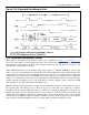
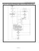
When data is to be read from data memory on the expanded bus, the external RD pin will be activated
during the second machine cycle of the MOVX instruction. A complete RD cycle, including activation of
ALE and RD, takes 12 clock oscillator periods. PSEN is inactive during this machine cycle. This cycle is
illustrated in Figure 15-5. When the MOVX instruction specifies a write operation to the external memory
device, the WR signal will be activated as shown in Figure 15-6. Data is output on Port 0 just before WR
is activated and remains valid until it goes back to its inactive level at the conclusion of the cycle.