
Datasheet


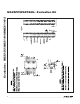


MAXSPCSPARTAN6+ Evaluation Kit
Evaluates: MAX5135/MAX11040/MAX11612
2 ______________________________________________________________________________________
Quick Start
The MAXSPCSPARTAN6+ board can be plugged in to
any Spartan 6 series FPGA evaluation board. A two-step
configuration is needed to use this card with the FPGA
evaluation board:
1) Place a shunt on pins 2-3 of header J7
(i.e., +3V3FMC to +3V3).
2) Place a shunt on pins 2-3 of header J6
(i.e., +5VREG to +5V).
Now connect the MAXSPCSPARTAN6+ board to the
FPGA EV kit. On power-up, LEDs D3, D4, and D5 should
glow, indicating a power-up state.
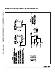
Detailed Description of Hardware
The MAXSPCSPARTAN6+ board is loaded with Maxim’s
ADCs and DACs and makes it very easy to integrate the
FPGA with any analog interface.
Communication with the MAX11612
The MAX11612 is a 12-bit, 2-/4-channel, I
2
C-compatible
ADC. The FPGA can drive commands for data
acquisition from the MAX11612 on the I
2
C slave address
0110100. The MAX11612 can work with the internal
reference of 4.096V or the external reference connected
at the AD3 port of J2. If internal reference is used; all
4 channels can be sampled from AD0–AD3. For more
information, refer to the MAX11612 IC data sheet.
Communication with the MAX11040
The MAX11040 is a 24-bit, 4-channel, SPI-compatible,
sigma-delta ADC with programmable output data rate.
It has an internal reference of 2.5V with Q2.2V input
range. Input ports are marked as AD0-/AD0+ to AD3-/
AD3+ on J3. External reference can also be applied. The
MAX11040 does simultaneous sampling and data for all
4 channels and can be acquired in one read.
This ADC has four standard connections for SPI
communication. It also has an extra signal (DRDYOUT)
that interrupts the FPGA at every end-of-conversion
to sample the data. For more information, refer to the
MAX11040 IC data sheet.
Communication with the MAX5135
The MAX5135 is a 12-bit, 4-channel, voltage output,
SPI-compatible DAC. The MAXSPCSPARTAN6+ board
contains two MAX5135 ICs in a cascaded configura-
tion. The DAC channels are marked as DA0–DA3 on J2
and DA4–DA7 on J3. For more information, refer to the
MAX5135 IC data sheet.
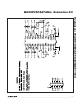
Table 1. MAXSPCSPARTAN6+ Connector
J2 Description
J2 PIN NO. LABEL FUNCTION
1 +5V
+5V, 250mA supply for external
circuit
2 N.C. Not connected
3 GND Ground
4 DA0
DAC output from channel 0 of U6
(MAX5135)
5 GND Ground
6 DA1
DAC output from channel 1 of U6
(MAX5135)
7 GND Ground
8 DA2
DAC output from channel 2 of U6
(MAX5135)
9 GND Ground
10 DA3
DAC output from channel 3 of U6
(MAX5135)
11 AD1
ADC input to channel 1 of U2
(MAX11612)
12 AD0
ADC input to channel 0 of U2
(MAX11612)
13 GND Ground
14 I/O
Digital input/output connected to
FMC connector at C18
15 AD3
ADC input to channel 3 of U2
(MAX11612)
16 AD2
ADC input to channel 2 of U2
(MAX11612)