
Datasheet


MAX9984
SiGe High-Linearity, 400MHz to 1000MHz
Downconversion Mixer with LO Buffer/Switch
2 _______________________________________________________________________________________
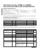
ABSOLUTE MAXIMUM RATINGS
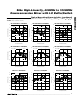
DC ELECTRICAL CHARACTERISTICS
(MAX9984 Typical Application Circuit, using component values in Table 1, V
CC
= +4.75V to +5.25V, no RF signal applied, IF+ and
IF- outputs pulled up to V
CC
through inductive chokes, R
1
= 953Ω, R
2
= 619Ω, T
C
= -40°C to +85°C, unless otherwise noted. Typical
values are at V
CC
= +5V, T
C
= +25°C, unless otherwise noted.)
Stresses beyond those listed under “Absolute Maximum Ratings” may cause permanent damage to the device. These are stress ratings only, and functional
operation of the device at these or any other conditions beyond those indicated in the operational sections of the specifications is not implied. Exposure to
absolute maximum rating conditions for extended periods may affect device reliability.
V
CC
to GND...........................................................-0.3V to +5.5V
IF+, IF-, LOBIAS, LOSEL, IFBIAS to GND...-0.3V to (V
CC
+ 0.3V)
TAP ........................................................................-0.3V to +1.4V
LO1, LO2, LEXT to GND........................................-0.3V to +0.3V
RF, LO1, LO2 Input Power .............................................+12dBm
RF (RF is DC shorted to GND through a balun) .................50mA
Continuous Power Dissipation (T
A
= +70°C)
20-Pin Thin QFN-EP (derate 26.3mW/°C above +70°C)...........2.1W
θ
JA
.................................................................................+38°C/W
θ
JC
.................................................................................+13°C/W
Operating Temperature Range (Note A) ....T
C
= -40°C to +85°C
Junction Temperature......................................................+150°C
Storage Temperature Range .............................-65°C to +150°C
Lead Temperature (soldering, 10s) .................................+300°C
Note A: T
C
is the temperature on the exposed paddle of the package.
PARAMETER SYMBOL CONDITIONS MIN TYP MAX UNITS
Supply Voltage V
CC
4.75 5.00 5.25 V
Supply Current I
CC
222 265 mA
LO_SEL Input-Logic Low V
IL
0.8 V
LO_SEL Input-Logic High V
IH
2V
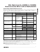
AC ELECTRICAL CHARACTERISTICS
(MAX9984 Typical Application Circuit, using component values in Table 1, V
CC
= +4.75V to +5.25V, RF and LO ports are driven from
50Ω sources, P
LO
= -3dBm to +3dBm, P
RF
= -5dBm, f
RF
= 815MHz to 1000MHz, f
LO
= 570MHz to 850MHz, f
IF
= 160MHz, f
RF
> f
LO
,
T
C
= -40°C to +85°C, unless otherwise noted. Typical values are at V
CC
= +5V, P
RF
= -5dBm, P
LO
= 0dBm, f
RF
= 910MHz, f
LO
=
750MHz, f
IF
= 160MHz, T
C
= +25°C, unless otherwise noted.) (Note 1)
PARAMETER SYMBOL CONDITIONS MIN TYP MAX UNITS
(Note 2) 815 1000
RF Frequency Range f
RF
(Notes 2, 3) 400
MHz
(Note 2) 570 850
(Notes 2, 3) 325
LO Frequency Range f
LO
MAX9986 960 1180
MHz
IF Frequency Range f
IF
(Note 2) 50 250 MHz
Conversion Gain G
C
f
RF
= 910MHz, f
LO
= 750MHz, T
C
= +25°C 7.2 8.1 9.2 dB
Gain Variation Over Temperature T
C
= -40°C to +85°C- 0.0079 dB/°C
Conversion Gain Flatness
Fl atness over any one of thr ee fr equency b and s:
f
RF
= 824MHz to 849MHz
f
RF
= 869MHz to 894MHz
f
RF
= 880MHz to 915MHz
±0.25 dB
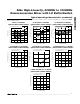
Input Compression Point P
1dB
(Note 4) 13 dBm
f
LO
= 570MHz to 850MHz, f
IF
= 160MHz,
P
LO
= 0dBm, T
C
= +25°C (Note 5)
19
Input Third-Order Intercept Point IIP3
Two tones:
f
RF1
= 910MHz, f
RF2
= 911MHz,
P
RF
= -5dBm/tone, f
LO
= 750MHz,
P
LO
= 0dBm, T
C
= +25°C
22 25
dBm