
Datasheet


MAX9984
SiGe High-Linearity, 400MHz to 1000MHz
Downconversion Mixer with LO Buffer/Switch
10 ______________________________________________________________________________________
Detailed Description
The MAX9984 high-linearity downconversion mixer
provides 8.1dB of conversion gain and +25dBm of
IIP3, with a typical 9.3dB noise figure. The integrated
baluns and matching circuitry allow for 50Ω single-
ended interfaces to the RF and the two LO ports. A sin-
gle-pole, double-throw (SPDT) switch provides 50ns
switching time between the two LO inputs with 54dB of
LO-to-LO isolation. Furthermore, the integrated LO
buffer provides a high drive level to the mixer core,
reducing the LO drive required at the MAX9984’s
inputs to a -3dBm to +3dBm range. The IF port incor-
porates a differential output, which is ideal for provid-
ing enhanced IIP2 performance.
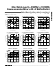
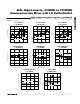
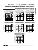
Specifications are guaranteed over broad frequency
ranges to allow for use in cellular band GSM,
cdma2000, iDEN, and W-CDMA 2G/2.5G/3G base sta-
tions. The MAX9984 is optimized to operate over a
815MHz to 1000MHz RF frequency range, a 570MHz to
850MHz LO frequency range, and a 50MHz to 250MHz
IF frequency range. Operation beyond these ranges is
possible; see the Typical Operating Characteristics for
additional details. For operation at a 400MHz to
500MHz RF frequency range, see the Typical
Operating Characteristics and Table 2 for details.
RF Input and Balun
The MAX9984 RF input is internally matched to 50Ω,
requiring no external matching components. A DC-
blocking capacitor is required because the input is inter-
nally DC shorted to ground through the on-chip balun.
LO Inputs, Buffer, and Balun
The MAX9984 is ideally suited for low-side LO injection
applications with an optimized 570MHz to 850MHz LO
frequency range. Appropriate tuning allows for an LO
frequency range below 570MHz (RF frequency below
815MHz). For a device with a 960MHz to 1180MHz LO
frequency range, refer to the MAX9986 data sheet. As
an added feature, the MAX9984 includes an internal LO
SPDT switch that can be used for frequency-hopping
applications. The switch selects one of the two single-
ended LO ports, allowing the external oscillator to settle
on a particular frequency before it is switched in. LO
switching time is typically less than 50ns, which is more
than adequate for virtually all GSM applications. If fre-
quency hopping is not employed, set the switch to
either of the LO inputs. The switch is controlled by a
digital input (LOSEL): logic-high selects LO2, logic-low
selects LO1. To avoid damage to the part, voltage must
be applied to V
CC
before digital logic is applied to
LOSEL. LO1 and LO2 inputs are internally matched to
50Ω, requiring only a 82pF DC-blocking capacitor.
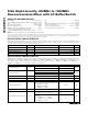
Pin Description
PIN NAME FUNCTION
1, 6, 8, 14 V
CC
Power-Supply Connection. Bypass each V
CC
pin to GND with capacitors as shown in the Typical
Application Circuit.
2RF
Single-Ended 50Ω RF Input. This port is internally matched and DC shorted to GND through a balun.
Requires an external DC-blocking capacitor.
3 TAP
Center Tap of the Internal RF Balun. Bypass to GND with capacitors close to the IC, as shown in the
Typical Application Circuit.
4, 5, 10, 12,
13, 17
GND Ground
7 LOBIAS Bias Resistor for Internal LO Buffer. Connect a 619Ω ±1% resistor from LOBIAS to the power supply.
9 LOSEL Local Oscillator Select. Logic control input for selecting LO1 or LO2.
11 LO1 Local Oscillator Input 1. Drive LOSEL low to select LO1.
15 LO2 Local Oscillator Input 2. Drive LOSEL high to select LO2.
16 LEXT
External Inductor Connection. Connect a low-ESR, 47nH inductor from LEXT to GND. This inductor
carries approximately 140mA DC current.
18, 19 IF-, IF+
Differential IF Outputs. Each output requires external bias to V
CC
through an RF choke (see the
Typical Application Circuit).
20 IFBIAS IF Bias Resistor Connection for IF Amplifier. Connect a 953Ω ±1% resistor from IFBIAS to GND.
EP GND Exposed Ground Paddle. Solder the exposed paddle to the ground plane using multiple vias.