
Datasheet


MAX9744
20W Stereo Class D Speaker Amplifier
with Volume Control
_______________________________________________________________________________________ 5
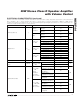
ELECTRICAL CHARACTERISTICS (continued)
(V
PVDD
= 12V, V
DD
= 3.3V, V
GND
= V
PGND
= 0V, V
MUTE
= 0V; max volume setting; all speaker load resistors connected between
OUT_+ and OUT_-, R
L
= ∞, unless otherwise stated, C
BOOT_
= 0.1µF, C
BIAS
= 2.2µF, C
IN
= 0.47µF, R
IN
= 20kΩ, R
F_
= 20kΩ, spread-
spectrum mode, filterless modulation mode, see the
Functional Diagrams/Typical Application Circuits.
T
A
= T
MIN
to T
MAX
, unless oth-
erwise noted. Typical values are at T
A
= +25°C.) (Note 1)
PARAMETER SYMBOL CONDITIONS MIN TYP MAX UNITS
DIGITAL INPUT (SYNC)
Input-Voltage High V
SYNCIH
2.3 V
Input-Voltage Low V
SYNCIL
0.8 V
SYNC Input Leakage I
SYNCIN
T
A
= +25°C ±7.5 ±13 µA
DIGITAL OUTPUT (SYNCOUT)
Output-Voltage High V
SYNCOUTIH
I
SOURCE
= 1mA
V
DD
-
0.3
V
Output-Voltage Low V
SYNCOUTIL
I
SINK
= 1mA 0.3 V
Rise/Fall Time C
L
= 10pF 50 V/µs
THERMAL PROTECTION
Thermal-Shutdown Threshold +165 °C
Thermal-Shutdown Hysteresis 15 °C
I
2
C TIMING CHARACTERISTICS (Figure 3)
Serial Clock f
SCL
400 kHz
Bus Free Time Between a STOP
and a START Condition
t
BUF
1.3 µs
Hold Time (Repeated) START
Condition
t
HD, STA
(Note 5) 0.6 µs
Repeated START Condition
Setup Time
t
SU, STA
0.6 µs
STOP Condition Setup Time t
SU, STO
0.6 µs
Data Hold Time t
HD,DAT
0 0.9 µs
Data Setup Time t
SU,DAT
100 ns
SCL Clock Low Period t
LOW
1.3 µs
SCL Clock High Period t
HIGH
0.6 µs
Rise Time of SDA and SCL,
Receiving
t
R
(Note 6)
20 +
0.1C
B
300 ns
Fall Time of SDA and SCL,
Receiving
t
F
(Note 6)
20 +
0.1C
B
300 ns
Pulse Width of Spike Suppressed t
SP
050ns
Capacitive Load for Each Bus
Line
C
B
400 pF
Note 1: All devices are 100% production tested at +25°C. All temperature limits are guaranteed by design.
Note 2: See the
Gain-Setting Resistors
section.
Note 3: Measured on the MAX9744 Evaluation Kit.
Note 4: Testing performed with an 8Ω resistive load connected across BTL output. Mode transitions are controlled by SHDN or
MUTE pin, respectively.
Note 5: A master device must provide a hold time of at least 300ns for the SDA signal in order to bridge the undefined region of the
SCL’s falling edge.
Note 6: C
B
= total capacitance of one bus line in pF.