
Datasheet


MAX9744
20W Stereo Class D Speaker Amplifier
with Volume Control
2 _______________________________________________________________________________________
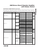
ABSOLUTE MAXIMUM RATINGS
ELECTRICAL CHARACTERISTICS
(V
PVDD
= 12V, V
DD
= 3.3V, V
GND
= V
PGND
= 0V, V
MUTE
= 0V; max volume setting; all speaker load resistors connected between
OUT_+ and OUT_-, R
L
= ∞, unless otherwise stated, C
BOOT_
= 0.1µF, C
BIAS
= 2.2µF, C
IN
= 0.47µF, R
IN
= 20kΩ, R
F_
= 20kΩ, spread-
spectrum mode, filterless modulation mode, see the
Functional Diagrams/Typical Application Circuits.
T
A
= T
MIN
to T
MAX
, unless oth-
erwise noted. Typical values are at T
A
= +25°C.) (Note 1)
Stresses beyond those listed under “Absolute Maximum Ratings” may cause permanent damage to the device. These are stress ratings only, and functional
operation of the device at these or any other conditions beyond those indicated in the operational sections of the specifications is not implied. Exposure to
absolute maximum rating conditions for extended periods may affect device reliability.
PVDD to PGND ....................................................................+16V
V
DD
to GND ...........................................................................+4V
FB_, SYNCOUT, SYNC, SDA/VOL, ADDR1,
ADDR2 to GND........................................-0.3V to (V
DD
+ 0.3V)
BOOT_ to V
DD
..........................................................-0.3V to +6V
BOOT_ to OUT_........................................................-0.3V to +6V
OUT_ to GND ..........................................-0.3V to (PVDD + 0.3V)
PGND to GND .......................................................-0.3V to +0.3V
Any Other Pin to GND ..............................................-0.3V to +4V
OUT_, Short-Circuit Duration......................................Continuous
Continuous Power Dissipation (T
A
= +70°C)
44-Pin Thin QFN (derate 27mW/°C above +70°C,
single-layer board) ...................................................2162mW
44-Pin Thin QFN (derate 37mW/°C above +70°C,
multilayer board) ......................................................2963mW
θ
JA
, Single-Layer Board................................................37°C/W
θ
JA
, Multilayer Board ................................................….27°C/W
Continuous Input Current (PVDD, PGND).............................6.4A
Continuous Output Current (OUT_) ......................................3.2A
Continuous Input Current (except OUT_).........................±20mA
Junction Temperature......................................................+150°C
Operating Temperature Range ...........................-40°C to +85°C
Storage Temperature Range .............................-65°C to +150°C
Lead Temperature (soldering, 10s) .................................+300°C
PARAMETER SYMBOL CONDITIONS MIN TYP MAX UNITS
GENERAL
Speaker Amplifier Supply Voltage
Range
PVDD Inferred from PSRR test 4.5 14 V
Supply Voltage Range V
DD
Inferred from PSRR test 2.7 3.6 V
I
DD
20 35
Quiescent Current
I
PVDD
10 20
mA
I
VDDSHDN
T
A
= +25°C 0.1 1
Shutdown Current
I
PVDDSHDN
T
A
= +25°C 0.1 1
µA
Turn-On Time t
ON
200 ms
Common-Mode Bias Voltage V
BIAS
1.5 V
Input Amplifier Output-Voltage
Swing High
V
OH
Specified as V
DD
– V
OH
, R
L
= 2kΩ
connected to 1.5V
20 mV
Input Amplifier Output-Voltage
Swing Low
V
OL
Specified as V
OL
– GND, R
L
= 2kΩ
connected to 1.5V
20 mV
Input Amplifier Output Short-
Circuit Current Limit
±60 mA
Input Amplifier Gain-Bandwidth
Product
GBW 1.8 MHz
SPEAKER AMPLIFIERS
Output stage gain 29.5
Gain A
VMAX
Maximum
volume setting
Total gain (Note 2) 29.5
dB
Output Offset V
OS
T
A
= 25°C ±2 ±15 mV