
Datasheet

MAX9736
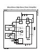
Mono/Stereo High-Power Class D Amplifier
______________________________________________________________________________________ 17
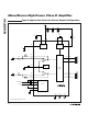
Internal Regulator
The MAX9736 features an internal 5V regulator, VS,
powered from PVDD. Connect REGEN to SHDN so that
the internal 5V regulator is enabled/disabled when the
MAX9736 is enabled/disabled. If an external 5V supply
is available, drive REGEN low and connect external 5V
supply to VS to minimize the power dissipation of the
MAX9736.
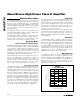
Supply Bypassing,
Layout, and Grounding
Proper layout and grounding are essential for optimum
performance. Use wide traces for the power-supply
inputs and amplifier outputs to minimize losses due to
parasitic trace resistance. Proper grounding improves
audio performance, minimizes crosstalk between chan-
nels, and prevents switching noise from coupling into
the audio signal. Connect PGND and AGND together at
a single point on the PCB. Route all traces that carry
switching transients away from AGND and the
traces/components in the audio signal path.
Bypass each PVDD pin with a 0.1μF capacitor to PGND.
Place the bypass capacitors as close as possible to the
MAX9736. Place a 220μF capacitor between PVDD and
PGND. Bypass VS with a 1μF capacitor to AGND.
Use wide, low-resistance output traces. Current drawn
from the outputs increases as load impedance
decreases. High-output trace resistance decreases the
power delivered to the load. The MAX9736 TQFN pack-
age features an exposed thermal paddle on its under-
side. This paddle lowers the package’s thermal
resistance by providing a heat conduction path from
the die to the PCB. Connect the exposed thermal pad
to PGND by using a large pad and multiple vias to the
PGND plane.