
Datasheet


MAX9242/MAX9244/MAX9246/MAX9254
21-Bit Deserializers with Programmable
Spread Spectrum and DC Balance
6 _______________________________________________________________________________________
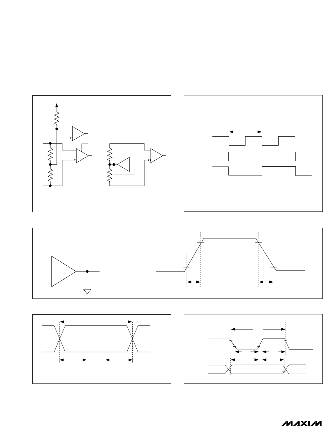
Test Circuits/Timing Diagrams
V
CC
- 0.3V
V
CC
R
IN2
R
IN1
RxIN_ + OR
RxCLKIN+
RxIN_ - OR
RxCLKIN-
R
IN1
R
IN1
RxIN_ + OR
RxCLKIN+
RxIN_ - OR
RxCLKIN-
R
IN1
FAIL-SAFE
COMPARATOR
DC-BALANCED MODENON-DC-BALANCED MODE
1.2V
Figure 1. LVDS Input Circuits
RCOP
RxCLKOUT
ODD RxOUT
EVEN RxOUT
Figure 2. Worst-Case Test Pattern
90%90%
10%10%
CHLTCLHT
RxOUT_ OR
RxCLKOUT
RxOUT_ OR
RxCLKOUT
8pF
Figure 3. Output Load and Transition Times
IDEAL
MIN MAX
INTERNAL STROBE
IDEAL
RSKM RSKM
IDEAL SERIAL BIT TIME
1.3V
1.1V
Figure 4. LVDS Receiver Input Skew Margin
RxOUT_
RxCLK OUT
RCOP
RCOHRCOL
2.0V
0.8V
2.0V
0.8V
2.0V
2.0V
2.0V
0.8V 0.8V
RHRCRSRC
Figure 5a. Rising-Edge Output Setup/Hold and High/Low Times