
Datasheet


MAX9242/MAX9244/MAX9246/MAX9254
21-Bit Deserializers with Programmable
Spread Spectrum and DC Balance
_______________________________________________________________________________________ 5
Note 1: Current into a pin is defined as positive. Current out of a pin is defined as negative. All voltages are referenced to ground,
except V
TH
and V
TL
.
Note 2: Maximum and minimum limits over temperature are guaranteed by design and characterization. Devices are production
tested at T
A
= +25°C.
Note 3: To provide a mid level, leave the input open, or, if driven, put driver in high impedance. High-impedance leakage current
must be less than ±10µA.
Note 4: RxCLKOUT limits are scaled based on RxOUT_ measurements, design, and characterization data.
Note 5: One output shorted at a time. Current out of the pin.
Note 6: V
TH
, V
TL
, and AC parameters are guaranteed by design and characterization, and are not production tested. Limits are set
at ±6 sigma.
Note 7: C
L
includes probe and test jig capacitance.
Note 8: RCIP is the period of RxCLKIN_. RCOP is the period of RxCLKOUT.
Note 9: RSKM is measured with less than 150ps cycle-to-cycle jitter on RxCLKIN_.
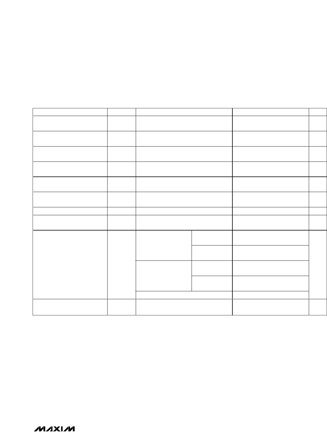
AC ELECTRICAL CHARACTERISTICS (continued)
(V
CC
= LVDSV
CC
= PLLV
CC
= +3.0V to +3.6V, V
CCO
= +3.0V to +3.6V, C
L
= 8pF, PWRDWN = high; SSG = high, open, or low;
DCB = high or low, differential input voltage |V
ID
| = 0.1V to 1.2V, input common-mode voltage V
CM
= |V
ID
/ 2| to 2.4V - |V
ID
/ 2|, unless
otherwise noted. Typical values are at V
CC
= V
CCO
= LVDSV
CC
= PLLV
CC
= +3.3V, |V
ID
| = 0.2V, V
CM
= +1.25V, T
A
= +25°C.) (Notes 6, 7, 8)
PARAMETER SYMBOL CONDITIONS MIN TYP MAX UNITS
RxCLKOUT High Time RCOH Figures 5a, 5b
0.35 x
RCOP
ns
RxCLKOUT Low Time RCOL Figures 5a, 5b
0.35 x
RCOP
ns
RxOUT_ Setup to RxCLKOUT RSRC Figures 5a, 5b
0.3 x
RCOP
ns
RxOUT_ Hold from RxCLKOUT RHRC Figures 5a, 5b
0.45 x
RCOP
ns
RxCLKIN_ to RxCLKOUT Delay RCCD SSG = low, Figures 6a, 6b
4.5 +
(RCIP / 2)
6.5 +
(RCIP / 2)
8.2 +
(RCIP / 2)
ns
Deserializer Phase-Locked-
Loop Set
RPLLS Figure 7
65,600 x
RCIP
ns
Deserializer Power-Down Delay RPDD Figure 8 100 ns
Deserializer Phase-Locked-
Loop Set from SSG Change
RPLLS2 Figure 9
32,800 x
RCIP
ns
M axi m um outp ut
fr eq uency
f
RxCLKIN_
+ 3.6%
f
RxCLKIN_
+ 4.0%
f
RxCLKIN_
+ 4.4%
SSG = high,
Figure 10
Minimum output
frequency
f
RxCLKIN_
- 4.4%
f
RxCLKIN_
- 4.0%
f
RxCLKIN_
- 3.6%
M axi m um outp ut
fr eq uency
f
RxCLKIN_
+ 1.8%
f
RxCLKIN_
+ 2.0%
f
RxCLKIN_
+ 2.2%
SSG = open,
Figure 10
Minimum output
frequency
f
RxCLKIN_
- 2.2%
f
RxCLKIN_
- 2.0%
f
RxCLKIN_
- 1.8%
Spread-Spectrum Output
Frequency
f
RxCLKOUT
SSG = low f
RxCLKIN_
f
RxCLKIN_
MHz
Spread-Spectrum Modulation
Frequency
f
SSM
Figure 10
f
RxCLKIN_
/
1016
Hz