
Datasheet


MAX9242/MAX9244/MAX9246/MAX9254
21-Bit Deserializers with Programmable
Spread Spectrum and DC Balance
______________________________________________________________________________________ 17
R
T
is required to match the transmission line impedance
(usually 100Ω) and R
O
is determined by the LVDS dri-
ver design (the minimum differential output resistance of
78Ω for the MAX9209/MAX9213 serializers is used in
the following example). This condition leaves the capac-
itor selection to change the system time constant.
In the following example, the capacitor value for a 2%
droop is calculated. Jitter due to this droop is then cal-
culated assuming a 1ns transition time:
C = -(2 x t
B
x DSV) / (ln (1 - D) x (R
T
+ R
O
)) (Eq 1)
where:
C = AC-coupling capacitor (F)
t
B
= bit time (s)
DSV = digital sum variation (integer)
ln = natural log
D = droop (% of signal amplitude)
R
T
= termination resistor (Ω)
R
O
= output resistance (Ω)
Equation 1 is for two series capacitors (Figure 19). The bit
time (t
B
) is the period of the parallel clock divided by 9.
The DSV is 10. See equation 3 for four series capacitors
(Figure 20).
The capacitor for 2% maximum droop at 16MHz parallel
rate clock is:
C = -(2 x t
B
x DSV) / (ln (1 - D) x (R
T
+ R
O
))
C = -(2 x 6.95ns x 10) / (ln (1 - 0.02) x (100Ω + 78Ω))
C = 0.038µF
Jitter due to droop is proportional to the droop and
transition time:
t
J
= t
T
x D (Eq 2)
where:
t
J
= jitter (s)
t
T
= transition time (s) (0 to 100%)
D = droop (% of signal amplitude)
Jitter due to 2% droop and assumed 1ns transition time is:
t
J
= 1ns x 0.02
t
J
= 20ps
The transition time in a real system depends on the fre-
quency response of the cable driven by the serializer.
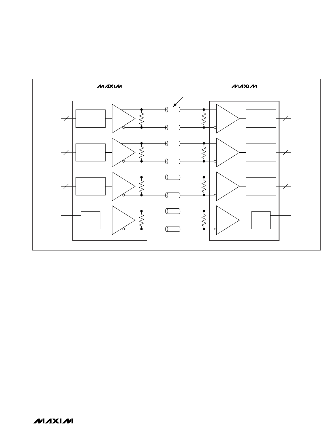
Figure 18. DC-Coupled Link, Non-DC-Balanced Mode
7:1
1:7 FIFO
7
7
100Ω
7:1
1:7 FIFO
7
7
100Ω
7:1
1:7 FIFO
7
7
100Ω
PLL
PLL1 +
SSPLL
100Ω
MAX9209/MAX9213 MAX9242/MAX9244/MAX9246/MAX9254
TxOUT
TxCLK OUT
RxIN__
RxCLK IN
21:3 SERIALIZER 3:21 DESERIALIZER
PWRDWN
RxCLK OUT
RxOUT_
PWRDWN
TxCLK IN
TxIN
TRANSMISSION LINE
R
O
R
T