
Datasheet


MAX9242/MAX9244/MAX9246/MAX9254
21-Bit Deserializers with Programmable
Spread Spectrum and DC Balance
To select the mid level, leave the input open, or if driven,
put the driver output in high impedance. The driver high-
impedance leakage current must be less than ±10µA.
Any spread change causes a maximum delay time of
32,800 x RCIP before output data is valid. When the
spread amount is changed from ±2% to ±4% or vice-
versa, the data outputs go low for one delay time (see
Figure 13). Similarly, when the spread is changed from
no spread to ±2% or ±4%, the data outputs go low for
one delay time (see Figure 14). The data outputs contin-
ue to switch but are not valid when the spread amount is
changed from ±2% or ±4% to no spread (see Figure
15). The spread-spectrum function is also available
when the MAX9242/MAX9244/MAX9246/MAX9254 oper-
ate in non-DC-balanced mode.
Hot Swap
When the MAX9242/MAX9244/MAX9246/MAX9254 are
connected to an active serializer, they synchronize correct-
ly. The PLL control voltage does not saturate in response to
high-frequency glitches that may occur during a hot swap.
The PWRDWN input on the MAX9242/MAX9244/MAX9246/
MAX9254 does not need to be cycled when these devices
are connected to an active serializer.
PLL Lock Time
The MAX9242/MAX9244/MAX9246/MAX9254 use two
PLLs. The first PLL (PLL1) generates a 7x clock (non-DC-
balanced mode) or a 9x clock (DC-balanced mode) from
RxCLKIN_ for deserializing the LVDS inputs. The second
PLL (SSPLL) is used for spread-spectrum modulation.
During initial power-up, the PLL1 locks, and SSPLL locks
immediately after. The PLL lock times are set by an inter-
nal counter. The maximum time to lock for each PLL is
32,800 clock periods. Power and clock should be stable
to meet the lock time specification. After initialization, if
the first PLL loses lock, it locks again and then the
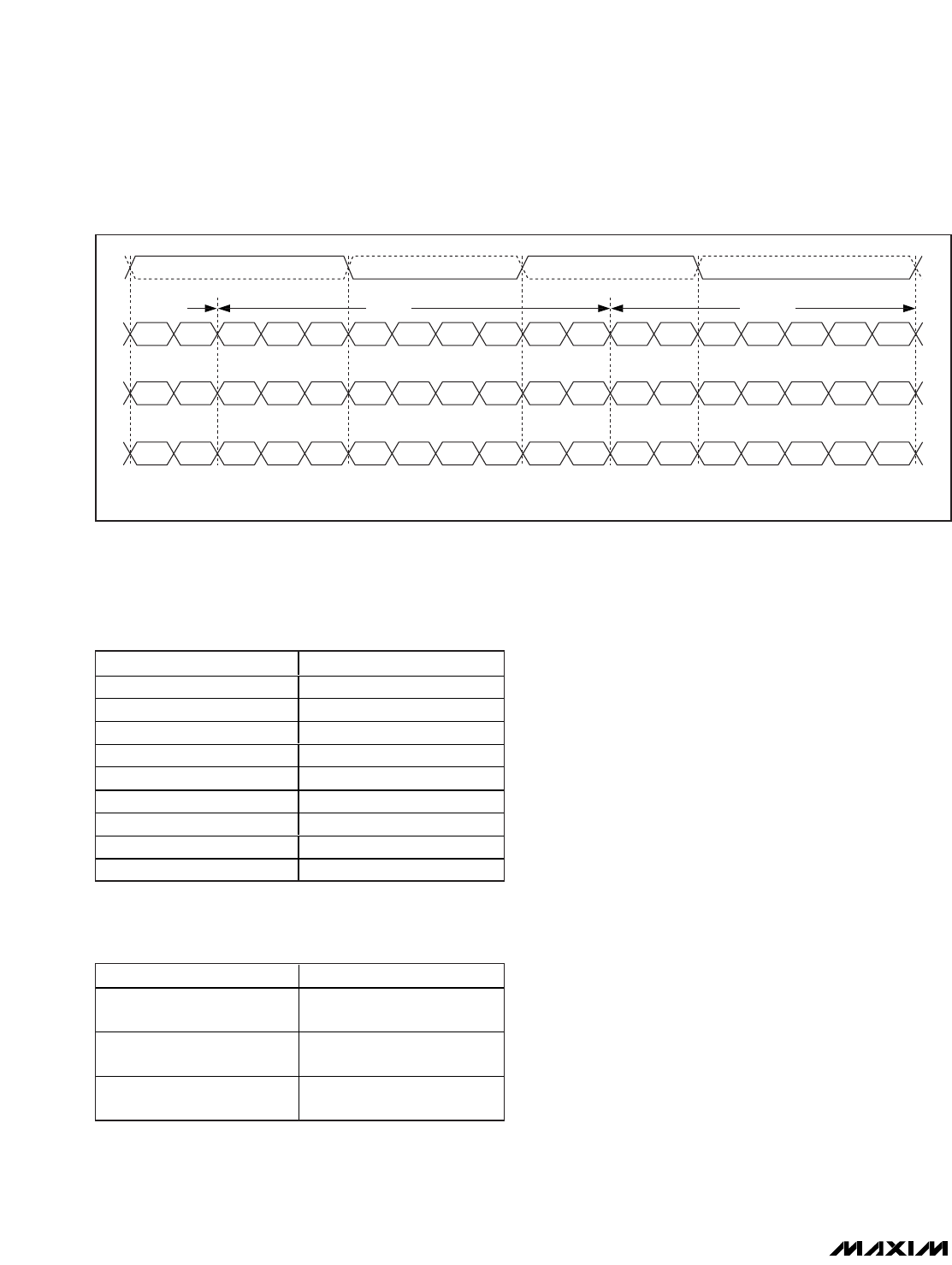
TxIN_, DCA_, AND DCB_ ARE DATA FROM THE SERIALIZER.
DCA0
DCB1DCA1
DCB2DCA2
CYCLE N + 1CYCLE NCYCLE N - 1
TxIN2TxIN6 TxIN3TxIN4TxIN5
TxIN9TxIN13 TxIN10TxIN11TxIN12
TxIN2TxIN3TxIN4DCA0 TxIN5TxIN6DCB0
TxIN9TxIN10TxIN11DCA1 TxIN12TxIN13DCB1
TxIN16TxIN17TxIN18DCA2 TxIN19TxIN20DCB2
TxIN0TxIN1
TxIN7TxIN8
TxIN14TxIN15TxIN16TxIN20 TxIN17TxIN18TxIN19
DCB0
RxCLKIN_
RxIN1_
RxIN0_
RxIN2_
TxIN1
TxIN8
TxIN15
TxIN0
TxIN7
TxIN14
+
-
Figure 12. Deserializer Serial Input in DC-Balanced Mode
Table 2. Modulation Rate
f
RxCLKIN_
(MHz) f
M
(kHz) = f
RxCLKIN
_
/ 1016
6 5.91
8 7.87
10 9.84
16 15.75
18 17.72
20 19.68
33 32.48
34 33.46
40 39.37
Table 3. SSG Function
SSG INPUT LEVEL FUNCTION
High
RxCLKOUT frequency spread
±4% relative to RxCLKIN_
Mid
RxCLKOUT frequency spread
±2% relative to RxCLKIN_
Low
No spread on RxCLKOUT
relative to RxCLKIN_
Note: RxOUT_ data outputs are spread because RxCLKOUT
strobes the output of the FIFO.
14 ______________________________________________________________________________________