
Datasheet
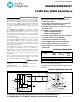


MAX9205/MAX9207
10-Bit Bus LVDS Serializers
2
Maxim Integrated
ABSOLUTE MAXIMUM RATINGS
DC ELECTRICAL CHARACTERISTICS
(V
AVCC
= V
DVCC
= +3.0V to +3.6V, R
L
= 27Ω ±1% or 50Ω ±1%, C
L
= 10pF, T
A
= -40°C to +85°C. Typical values are at V
AVCC
=
V
DVCC
= +3.3V and T
A
= +25°C, unless otherwise noted.) (Notes 2, 3, 4)
Stresses beyond those listed under “Absolute Maximum Ratings” may cause permanent damage to the device. These are stress ratings only, and functional
operation of the device at these or any other conditions beyond those indicated in the operational sections of the specifications is not implied. Exposure to
absolute maximum rating conditions for extended periods may affect device reliability.
AVCC, DVCC to GND..........................……………-0.3V to +4.0V
IN_, SYNC1, SYNC2, EN, TCLK_R/F, TCLK,
PWRDN to GND......................................-0.3V to (V
CC
+ 0.3V)
OUT+, OUT- to GND .............................................-0.3V to +4.0V
Output Short-Circuit Duration.....................................Continuous
Continuous Power Dissipation (T
A
= +70°C)
28-Pin SSOP (derate 9.5mW/°C above +70°C) ..........762mW
Storage Temperature Range .............................-65°C to +150°C
Junction Temperature......................................................+150°C
Operating Temperature Range ...........................-40°C to +85°C
ESD Protection (Human Body Model, OUT+, OUT-) ...........±8kV
Lead Temperature (soldering, 10s) .................................+300°C
Soldering Temperature (reflow) .......................................+260°C
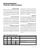
PARAMETER SYMBOL CONDITIONS MIN TYP MAX UNITS
LVCMOS/LVTLL LOGIC INPUTS (IN0 TO IN9, EN, SYNC1, SYNC2, TCLK, TCLK_R/F, PWRDN)
High-Level Input Voltage V
IH
2.0 V
CC
V
Low-Level Input Voltage V
IL
GND 0.8 V
Input Current I
IN
V
IN_
= 0V or V
_VCC
-20 +20 µA
BUS LVDS OUTPUTS (OUT+, OUT-)
R
L
= 27Ω 200 286 400 mV
Differential Output Voltage V
OD
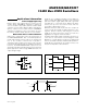
Figure 1
R
L
= 50Ω 250 460 600 mV
Change in V
OD
Between
Complementary Output States
∆V
OD
Figure 1 1 35 mV
Output Offset Voltage V
OS
Figure 1 0.9 1.15 1.3 V
Change in V
OS
Between
Complementary Output States
∆V
OS
Figure 1 3 35 mV
Output Short-Circuit Current I
OS
V
OUT+
or V
OUT-
= 0V,
IN0 to IN9 = PWRDN = EN = high
-13 -15 mA
Output High-Impedance Current I
OZ
V
PWRDN
or V
EN
= 0.8V,
V
OUT+
or V
OUT-
= 0V or V
_VCC
-10 +10 µA
Power-Off Output Current I
OX
V
_VCC
= 0V, V
OUT+
or V
OUT-
= 0V or 3.6V -10 +10 µA
POWER SUPPLY
16MHz 23 35
MAX9205
40MHz 34 45
40MHz 32 50
Supply Current I
CC
R
L
= 27_ or 50_
worst-case pattern
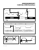
(Figures 2, 4)
MAX9207
66MHz 45 60
mA
Power-Down Supply Current I
CCX
PWRDN = low 8 mA
Note 1: Package thermal resistances were obtained using the method described in JEDEC specification JESD51-7, using a four-layer
board. For detailed information on package thermal considerations, refer to www.maximintegrated.com/thermal-tutorial
.
PACKAGE THERMAL CHARACTERISTICS (Note 1)
SSOP
Junction-to-Ambient Thermal Resistance (θ
JA
)...............68°C/W
Junction-to-Case Thermal Resistance (θ
JC
)......................25°C/W