
Datasheet


MAX9205/MAX9207
10-Bit Bus LVDS Serializers
12
Maxim Integrated
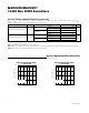
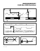
28
27
26
25
24
23
22
21
20
19
18
17
16
15
1
2
3
4
5
6
7
8
9
10
11
12
13
14
TOP VIEW
MAX9205
MAX9207
SYNC1
SYNC2
IN0
IN1
IN2
IN3
TCLK
IN4
IN5
IN6
IN7
IN8
IN9
TCLK_R/F
DGND
DGND
AVCC
AGND
EN
AGND
OUT-
OUT+
AGND
PWRDN
AGND
AVCC
DVCC
DVCC
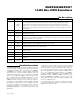
+
SSOP
OUT+
OUT-
EN
10
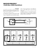
IN_
TCLK_R/F
TCLK
SYNC 1
SYNC 2
PLL
INPUT LATCH
PARALLEL-TO-SERIAL
TIMING AND
CONTROL
PWRDN
MAX9205
MAX9207
Functional DiagramPin Configuration
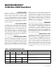
54Ω
ASIC
ASIC ASIC ASIC ASIC
54Ω
MAX9205
MAX9207
MAX9205
MAX9207
MAX9206
MAX9208
MAX9206
MAX9208
MAX9206
MAX9208
Figure 14. Multipoint
Chip Information
PROCESS: CMOS
Package Information
For the latest package outline information and land patterns (foot-
prints), go to www.maximintegrated.com/packages
. Note that a
“+”, “#”, or “-” in the package code indicates RoHS status only.
Package drawings may show a different suffix character, but the
drawing pertains to the package regardless of RoHS status.
PACKAGE
TYPE
PACKAGE
CODE
OUTLINE NO.
LAND
PATTERN NO.
28 SSOP A28+4
21-0056
90-0095