
Datasheet


MAX9153/MAX9154
Low-Jitter, 800Mbps, 10-Port LVDS
Repeaters with 100
Ω
Drive
_______________________________________________________________________________________ 7
impedance (to ground) when PWRDN = low or the
device is not powered. The outputs have a typical dif-
ferential resistance of 238Ω. The internal differential
output resistance terminates induced noise and reflec-
tions from the primary termination located at the LVDS
receiver.
The MAX9153/MAX9154 current-steering output
requires a resistive load to terminate the signal and
complete the transmission loop. Because the devices
switch the direction of current flow and not voltage lev-
els, the output voltage swing is determined by the value
of the termination resistor multiplied by the output cur-
rent. With a typical 3.8mA output current, the
MAX9153/MAX9154 produce a 380mV output voltage
when driving a transmission line terminated with a 100Ω
resistor (3.8mA x 100Ω = 380mV). Logic states are
determined by the direction of current flow through the
termination resistor.
Fail-Safe
The fail-safe feature of the MAX9153 sets the outputs
high when the differential input is:
• Open
• Undriven and shorted
• Undriven and terminated
Without a fail-safe circuit, when the input is undriven,
noise at the input may switch the outputs and it may
appear to the system that data is being sent. Open or
undriven terminated input conditions can occur when a
cable is disconnected or cut, or when an LVDS driver
output is in high impedance. A shorted input can occur
because of a cable failure.
When the input is driven with signals meeting the LVDS
standard, the input common-mode voltage is less than
V
CC
- 0.3V and the fail-safe circuit is not activated. If
the input is open, undriven and shorted, or undriven
and parallel terminated, an internal resistor in the fail-
safe circuit pulls both inputs above V
CC
- 0.3V, activat-
ing the fail-safe circuit and forcing the outputs high
(Figure 1).
The MAX9154 is essentially the MAX9153 without the
fail-safe circuit. The MAX9154 accepts input voltages
from 0 to V
CC
(vs. 0 to 2.4V for the MAX9153), which
allows interfacing to LVPECL input signals while retain-
ing a good common-mode tolerance.
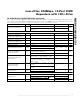
Table 1. Input/Output Function Table
Note: V
ID
= RIN+ - RIN-, V
OD
= DO_+ - DO_-
High = 450mV > V
OD
> 250mV
Low = -250mV > V
OD
> -450mV
MAX9153
V
CC
R
IN2
V
CC
- 0.3V
COMPARATOR
R
IN1
/2
R
IN1
/2
RIN+
RIN-
RECEIVER
DO1+
DO1-
DO10+
DO10-
Figure 1. MAX9153 Input Fail-Safe Circuit
MAX9154
R
IN3
R
IN3
RIN+
RIN-
DO1+
DO1-
DO10+
DO10-
V
CC
RECEIVER
Figure 2. MAX9154 Input Bias Resistors
INPUT, V
ID
OUTPUTS, V
OD
+50mV High
-50mV Low
Open
MAX9153
MAX9154
High
Undriven short MAX9153 High
Undriven terminated MAX9153 High