
Datasheet


MAX9153/MAX9154
Low-Jitter, 800Mbps, 10-Port LVDS
Repeaters with 100
Ω
Drive
4 _______________________________________________________________________________________
Note 1: Current into a pin is defined as positive. Current out of a pin is defined as negative. All voltages are referenced
to ground except V
TH
, V
TL
, V
ID
, V
OD
, and ΔV
OD
.
Note 2: Maximum and minimum limits over temperature are guaranteed by design and characterization. Devices are
production tested at T
A
= +25°C.
Note 3: Guaranteed by design and characterization.
Note 4: C
L
includes scope probe and test jig capacitance.
Note 5: Signal generator conditions unless otherwise noted: frequency = 400MHz, 50% duty cycle, R
O
= 50Ω, t
R
= 0.6ns,
and t
F
= 0.6ns (0% to 100%).
Note 6: Device jitter added to the input signal.
Note 7: t
CCS
is the magnitude difference in differential propagation delay between outputs for a same-edge transition.
Note 8: t
PPS1
is the magnitude difference of any differential propagation delays between devices operating over rated
conditions at the same supply voltage, input conditions, and ambient temperature.
Note 9: T
PPS2
is the magnitude difference of any differential propagation delays between devices operating over rated conditions.
Note 10: Device meets V
OD
DC specification, and AC specifications while operating at f
MAX
.
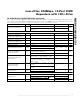
AC ELECTRICAL CHARACTERISTICS
(V
CC
= +3.0V to +3.6V, R
L
= 100Ω ±1%, C
L
= 5pF, differential input voltage |V
ID
| = 0.15V to 1.2V, MAX9153 LVDS input common-
mode voltage V
CM
= |V
ID
/2| to 2.4V - |V
ID
/2|, MAX9154 LVPECL input voltage range = 0 to V
CC
, PWRDN = high, T
A
= -40°C to +85°C,
unless otherwise noted. Typical values are at V
CC
= +3.3V, |V
ID
| = 0.2V, V
CM
= 1.2V, T
A
= +25°C.) (Notes 3, 4, 5)
PARAMETER SYMBOL CONDITIONS MIN TYP MAX UNITS
Rise Time t
LHT
150 220 450 ps
Fall Time t
HLT
Figures 4, 5
150 220 450 ps
400Mbps (NRZ) 13 50
Added Deterministic Jitter
(Note 6)
t
DJ
V
ID
= 200mV, 2
23
- 1
PRBS data, V
CM
= 1.2V
800Mbps (NRZ) 24 90
ps
(p-p)
200MHz 1
Added Random Jitter (Note 6) t
RJ
V
ID
= 200mV, 50% duty
cycle input, V
CM
= 1.2V
400MHz 1
ps
(RMS)
Differential Propagation Delay
Low to High
t
PLHD
1.6 2.3 3.3
Differential Propagation Delay
High to Low
t
PHLD
Figures 4, 5
1.6 2.3 3.3
ns
Pulse Skew | t
PLHD
- t
PHLD
|t
SKEW
Figures 4, 5 27 80 ps
Channel-to-Channel Skew
(Note 7)
t
CCS
Figures 4, 5 35 60 ps
Differential Part-to-Part Skew 1
(Note 8)
t
PPS1
1.2 ns
Differential Part-to-Part Skew 2
(Note 9)
t
PPS2
Figures 4, 5
1.7 ns
Maximum Input Frequency
(Note 10)
f
MAX
Figures 4, 5 800 Mbps
Power-Down Time t
PD
10 20 ns
Power-Up Time t
PU
Figures 6, 7
20 40 µs