
Datasheet


Board Layout
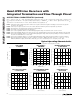
Because the MAX9121/MAX9122 feature a flow-through
pinout, no special layout precautions are required.
Keep the LVDS and any other digital signals separated
from each other to reduce crosstalk.
For LVDS applications, a four-layer PC board that pro-
vides separate power, ground, LVDS signals, and input
signals is recommended. Isolate the input LVDS signals
from each other to prevent coupling. Isolate the output
LVCMOS/LVTTL signals from each other to prevent
coupling. Separate the input LVDS signals from the out-
put signals planes with the power and ground planes
for best results.
MAX9121/MAX9122
Quad LVDS Line Receivers with
Integrated Termination and Flow-Through Pinout
_______________________________________________________________________________________ 9
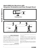
IN_+
EN
EN
IN_-
OUT_
DEVICE
UNDER
TEST
1/4 MAX9121/MAX9122
C
L
INCLUDES LOAD AND TEST JIG CAPACITANCE.
S
1
= V
CC
FOR t
PZL
AND t
PLZ
MEASUREMENTS.
S
1
= GND FOR t
PZH
AND t
PHZ
MEASUREMENTS.
GENERATOR
50Ω
C
L
R
L
S
1
V
CC
Figure 4. High-Impedance Delay Test Circuit
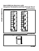
Figure 5. High-Impedance Delay Waveforms
1.5V
EN WHEN EN = GND OR OPEN
EN WHEN EN = V
CC
OUTPUT WHEN
V
ID
= -100mV
OUTPUT WHEN
V
ID
= +100mV
1.5V
1.5V
0.5V
0.5V
t
PLZ
t
PHZ
t
PZL
t
PZH
1.5V
3V
0
3V
V
CC
V
OL
V
OH
GND
0
50%
50%
Chip Information
TRANSISTOR COUNT: 1354
PROCESS: CMOS