
Datasheet


MAX9121/MAX9122
Quad LVDS Line Receivers with
Integrated Termination and Flow-Through Pinout
4 _______________________________________________________________________________________
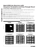
Typical Operating Characteristics
(V
CC
= +3.3V, V
CM
= +1.2V, |V
ID
| = 0.2V, C
L
= 15pF, T
A
= +25°C, unless otherwise noted.) (Figures 2 and 3)
40
0
0.01 0.1 1000100
SUPPLY CURRENT
vs. FREQUENCY
10
20
30
MAX9121/22 toc01
FREQUENCY (MHz)
SUPPLY CURRENT (mA)
110
ALL
CHANNELS
SWITCHING
ONE
SWITCHING
7.00
7.50
8.00
8.50
9.00
9.50
10.00
10.50
11.00
-40 -15 10 35 60 85
SUPPLY CURRENT vs.
TEMPERATURE
MAX9121/22 toc02
TEMPERATURE (°C)
SUPPLY CURRENT (mA)
0
10
30
20
40
50
3.0 3.3 3.6
DIFFERENTIAL THRESHOLD VOLTAGE
vs. SUPPLY VOLTAGE
MAX9121/22 toc03
SUPPLY VOLTAGE (V)
DIFFERENTIAL THRESHOLD VOLTAGE (mV)
Note 1: Current into a pin is defined as positive. Current out of a pin is defined as negative. All voltages are referenced to ground
except V
TH
, V
TL
, and V
ID
.
Note 2: Short only one output at a time. Do not exceed the absolute maximum junction temperature specification.
Note 3: AC parameters are guaranteed by design and characterization.
Note 4: C
L
includes scope probe and test jig capacitance.
Note 5: t
SKD1
is the magnitude difference of differential propagation delays in a channel. t
SKD1
= |t
PHLD
- t
PLHD
|.
Note 6: t
SKD2
is the magnitude difference of the t
PLHD
or t
PHLD
of one channel and the t
PLHD
or t
PHLD
of any other channel on the same part.
Note 7: t
SKD3
is the magnitude difference of any differential propagation delays between parts operating over rated conditions at
the same V
CC
and within 5°C of each other.
Note 8: t
SKD4
is the magnitude difference of any differential propagation delays between parts operating over rated conditions.
Note 9: f
MAX
generator output conditions: rise-time = fall-time = 1ns (0% to 100%), 50% duty cycle, V
OH
= +1.3V, V
OL
= +1.1V,
MAX9121/MAX9122 output criteria: 60% to 40% duty cycle, V
OL
= 0.4V (max), V
OH
= 2.7V (min), load = 15pF.
3.0 3.3 3.6
OUTPUT SHORT-CIRCUIT CURRENT
vs. SUPPLY VOLTAGE
MAX9121/22 toc04
SUPPLY VOLTAGE (V)
OUTPUT SHORT-CIRCUIT CURRENT (mA)
-70
-75
-80
-65
-90
-95
-85
1.30
1.25
1.20
1.15
1.10
3.0 3.3 3.6
OUTPUT HIGH-IMPEDANCE CURRENT
vs. SUPPLY VOLTAGE
MAX9121/22 toc05
SUPPLY VOLTAGE (V)
OUTPUT HIGH-IMPEDANCE CURRENT (nA)
2.7
2.9
3.3
3.1
3.5
3.7
3.0 3.3 3.6
OUTPUT HIGH VOLTAGE vs.
SUPPLY VOLTAGE
MAX9121/22 toc06
SUPPLY VOLTAGE (V)
OUTPUT HIGH VOLTAGE (V)
AC ELECTRICAL CHARACTERISTICS (continued)
(V
CC
= +3.0V to +3.6V, C
L
= 15pF, differential input voltage |V
ID
| = 0.2V to 1.0V, common-mode voltage V
CM
= |V
ID
/2| to 2.4V -
|V
ID
/2|, input rise and fall time = 1ns (20% to 80%), input frequency = 100MHz, T
A
= -40°C to +85°C. Typical values are at V
CC
=
+3.3V, V
CM
= 1.2V, |V
ID
| = 0.2V, T
A
= +25°C, unless otherwise noted.) (Notes 3, 4)