
Datasheet


MAX900–MAX903
High-Speed, Low-Power Voltage Comparators
2 _______________________________________________________________________________________
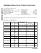
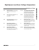
ABSOLUTE MAXIMUM RATINGS
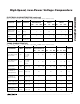
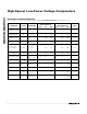
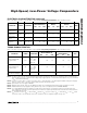
ELECTRICAL CHARACTERISTICS
(V
CC
= +5V, V
EE
= -5V, V
DD
= +5V, LE1–LE4 = logic high, T
A
= +25°C, unless otherwise noted.)
Stresses beyond those listed under “Absolute Maximum Ratings” may cause permanent damage to the device. These are stress ratings only, and functional
operation of the device at these or any other conditions beyond those indicated in the operational sections of the specifications is not implied. Exposure to
absolute maximum rating conditions for extended periods may affect device reliability.
Analog Supply Voltage (V
CC
to V
EE
) ...................................+12V
Digital Supply Voltage (V
DD
to GND) ....................................+7V
Differential Input Voltage..................(V
EE
- 0.2V) to (V
CC
+ 0.2V)
Common-Mode Input Voltage..........(V
EE
- 0.2V) to (V
CC
+ 0.2V)
Latch-Input Voltage (MAX900/MAX902/
MAX903 only) .........................................-0.2V to (V
DD
+ 0.2V)
Output Short-Circuit Duration
To GND.......................................................................Indefinite
To V
DD
...............................................................................1min
Internal Power Dissipation................................................500mW
Derate above +100°C ................................................10mW/°C
Operating Temperature Ranges:
MAX900–MAX903_C_ _ .......................................0°C to +70°C
MAX900–MAX903_E_ _ ....................................-40°C to +85°C
Junction Temperature........................................-65°C to +160°C
Storage Temperature Range .............................-65°C to +150°C
Lead Temperature (soldering, 10s) .................................+300°C
MAX900A/MAX901A
MAX900B/MAX901B/
MAX902/MAX903
PARAMETER SYMBOL CONDITIONS
MIN TYP MAX MIN TYP MAX
UNITS
Input Offset Voltage V
OS
V
CM
= 0
V
O
= 1.4V
0.5 2.0 1.0 4.0 mV
Input Bias Current I
B
I
IN
+ or I
IN
- 3 6 4 10 µA
Input Offset Current I
OS
V
CM
= 0;
V
O
= 1.4V
50 250 100 500 nA
Input Voltage Range V
CM
(Note 1) V
EE
- 0.1
V
CC
-
2.25
V
EE
- 0.1
V
CC
-
2.25
V
Common-Mode Rejection
Ratio
CMRR
-5V < V
CM
<
+2.75V,
V
O
= 1.4V
(Note 2)
50 150 75 250 µV/V
Power-Supply Rejection
Ratio
PSRR (Note 2) 50 150 100 250 µV/V
Output High Voltage V
OH
V
IN
> 250mV,
I
SRC
= 1mA
2.4 3.5 2.4 3.5 V
Output Low Voltage V
OL
V
IN
> 250mV,
I
SINK
= 8mA
0.3 0.4 0.3 0.4 V
Latch-Input Voltage High V
LH
(Note 3) 1.4 2.0 1.4 2.0 V
Latch-Input Voltage Low V
LL
(Note 3) 0.8 1.4 0.8 1.4 V
Latch-Input Current High I
LH
V
LH
= 3.0V
(Note 3)
1 20 1 20 µA
Latch-Input Current Low I
LL
V
LL
= 0.3V
(Note 3)
1 20 1 20 µA