
Datasheet


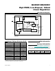

High PSRR, Low-Dropout, 150mA
Linear Regulators
Maxim Integrated 5
MAX8891/MAX8892
Detailed Description
The MAX8891/MAX8892 are low-dropout, low-quies-
cent current linear regulators designed for space-
restricted applications. The parts are available with
preset output voltages ranging from 1.5V to 4.5V in
100mV increments. These devices can supply loads up
to 150mA. As shown in the
Functional Diagram
, the
MAX8891 consists of an innovative bandgap core, error
amplifier, p-channel pass transistor, and internal feed-
back voltage-divider. The MAX8892 allows for
adjustable output with an external feedback network.
Additional blocks include a current limiter, thermal sen-
sor, and shutdown logic.
The 1.225V bandgap reference is connected to the
error amplifier’s inverting input. The error amplifier com-
pares this reference with the feedback voltage and
amplifies the difference. If the feedback voltage is lower
than the reference voltage, the pass-transistor gate is
pulled low. This allows more current to pass to the out-
put and increases the output voltage. If the feedback
voltage is too high, the pass transistor gate is pulled
high, allowing less current to pass to the output. The
output voltage is fed back through an internal (external
for the MAX8892) resistor voltage-divider connected to
the OUT pin.
Internal P-Channel Pass Transistor
The MAX8891/MAX8892 feature a 1Ω (typ) p-channel
MOSFET pass transistor. This provides several advan-
tages over similar designs using a PNP pass transistor,
including longer battery life. The p-channel MOSFET
requires no base drive, which considerably reduces qui-
escent current. PNP-based regulators waste consider-
able current in dropout when the pass transistor
saturates. They also use high base-drive current under
heavy loads. The MAX8891/MAX8892 do not suffer from
these problems and consume only 40µA of quiescent
current in light load and 220µA in dropout (see the
Typical Operating Characteristics
).
Output Voltage Selection
The MAX8891 is supplied with factory-set output volt-
ages from 1.5V to 4.5V, in 100mV increments (see the
Ordering Information
). The MAX8892 features a user-
adjustable output through an external feedback net-
work (see the
Typical Operating Circuits
).
To set the output of the MAX8892, use the following
equation:
where R2 is chosen to be less than 240kΩ and V
REF
=
1.225V. Use 1% or better resistors.
Shutdown
The MAX8891/MAX8892 feature a low-power shutdown
mode that reduces quiescent current less than 1µA.
Driving SHDN low disables the voltage reference, error
amplifier, gate-drive circuitry, and pass transistor (see
the
Functional Diagram
), and the device output enters a
high-impedance state. Connect SHDN to IN for normal
operation.
Current Limit
The MAX8891/MAX8892 include a current limiter, which
monitors and controls the pass transistor’s gate volt-
age, limiting the output current to 200mA. The output
can be continuously shorted to ground without damag-
ing the part.
RR
V
V
OUT
REF
12 1=×
⎛
⎝
⎜
⎞
⎠
⎟
-
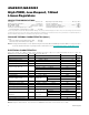
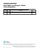
Pin Description
PIN
MAX8891
MAX8892
NAME FUNCTION
1 1 IN Unregulated Input Supply
2 2 GND Ground
33SHDN Shutdown. Pull low to disable the regulator.
— 4 FB Adjustable Output Feedback Point
4 — N.C. Not Internally Connected
5 5 OUT
Reg ul ated Outp ut V ol tag e. Byp ass w i th a cap aci tor to GN D . S ee the C ap aci tor S el ecti on
and Reg ul ator S tab i l i ty secti on for m or e d etai l s.