
Datasheet
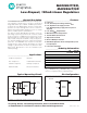


MAX8863T/S/R, MAX8864T/S/R
Low-Dropout, 120mA Linear Regulators
2
Maxim Integrated
ABSOLUTE MAXIMUM RATINGS
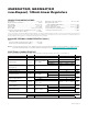
ELECTRICAL CHARACTERISTICS
(V
IN
= +3.6V, V
GND
= 0V, T
A
= T
MIN
to T
MAX
, unless otherwise noted. Typical values are at T
A
= +25°C.) (Note 2)
Stresses beyond those listed under “Absolute Maximum Ratings” may cause permanent damage to the device. These are stress ratings only, and functional
operation of the device at these or any other conditions beyond those indicated in the operational sections of the specifications is not implied. Exposure to
absolute maximum rating conditions for extended periods may affect device reliability.
V
IN
to GND ..................................................................-7V to +7V
Output Short-Circuit Duration ............................................Infinite
SET to GND ..............................................................-0.3V to +7V
SHDN to GND..............................................................-7V to +7V
SHDN to IN ...............................................................-7V to +0.3V
OUT to GND ................................................-0.3V to (V
IN
+ 0.3V)
Continuous Power Dissipation (multilayer board, T
A
= +70°C)
SOT23 (3.9mW/°C above +70°C).............................312.6mW
Operating Temperature Range ...........................-40°C to +85°C
Operating Temperature
Range (MAX8863TMUK/PR3+).....................-55°C to +125°C
Junction Temperature......................................................+150°C
Storage Temperature Range .............................-65°C to +150°C
Lead Temperature (soldering, 10s) .................................+300°C
Soldering Temperature (reflow) .......................................+260°C
Note 1: Package thermal resistances were obtained using the method described in JEDEC specification JESD51-7, using a four-layer
board. For detailed information on package thermal considerations, refer to www.maximintegrated.com/thermal-tutorial
.
PACKAGE THERMAL CHARACTERISTICS (Note 1)
SOT23
Junction-to-Ambient Thermal Resistance (θ
JA
)...............255.9°C/W
Junction-to-Case Thermal Resistance (θ
JC
)......................81°C/W
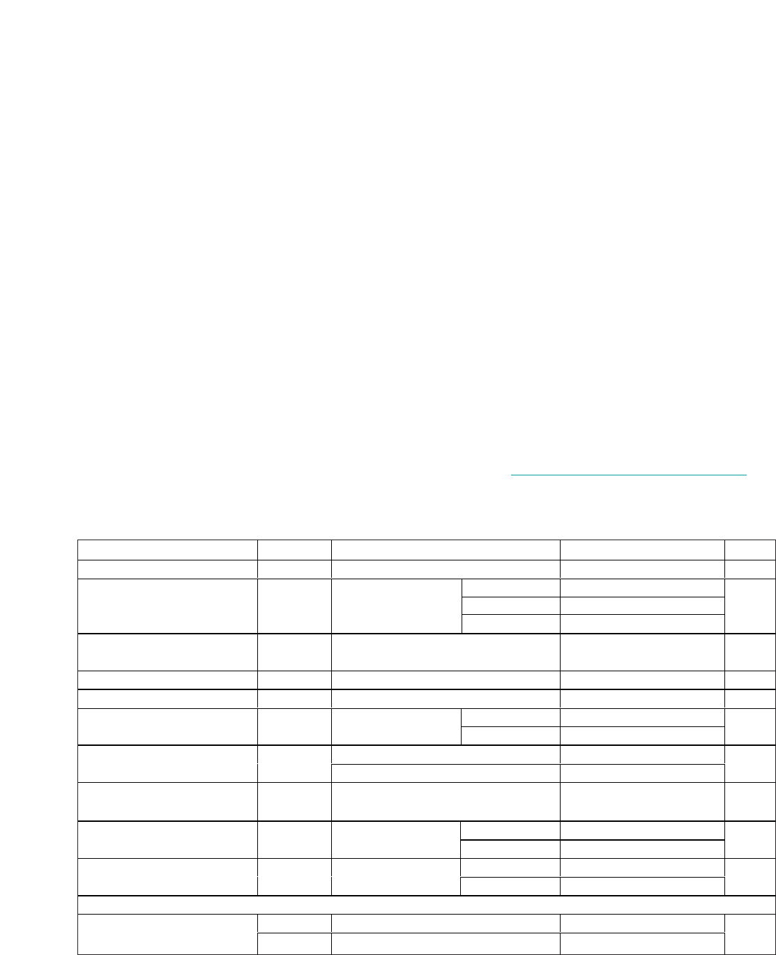
PARAMETER SYMBOL CONDITIONS MIN TYP MAX UNITS
Input Voltage (Note 3) V
IN
2.5 6.5 V
MAX886_T 3.05 3.15 3.25
MAX886_S 2.75 2.84 2.93Output Voltage V
OUT
0mA ≤ I
OUT
≤ 50mA,
SET = GND
MAX886_R 2.70 2.80 2.88
V
Adjustable Output Voltage
Range (Note 4)
V
OUT
V
SET
6.5 V
Maximum Output Current 120 mA
Current Limit (Note 5) I
LIM
280 mA
I
LOAD
= 0mA 68 150
Ground Pin Current I
Q
SET = GND
I
LOAD
= 50mA 80
µA
I
OUT
= 1mA 1.1
D r op out V ol tag e ( N ote 6)
I
OUT
= 50mA 55 120
mV
Line Regulation ΔV
LNR
V
IN
= 2.5V to 6.5V, SET tied to OUT,
I
OUT
= 1mA
-0.15 0 +0.15 %/V
SET = GND 0.011 0.040
Load Regulation ΔV
LDR
I
OUT
= 0mA to 50mA
S E T ti ed to O U T 0.006
%/mA
C
OUT
= 1µF 350
Output Voltage Noise 10Hz to 1MHz
C
OUT
= 100µF 220
µV
RM S
SHUTDOWN
V
IH
2.0
SHDN Input Threshold
V
IL
0.4
V