
Datasheet

MAX8662/MAX8663
Power-Management ICs for
Single-Cell, Li+ Battery-Operated Devices
_______________________________________________________________________________________ 7
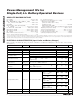
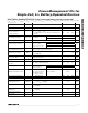
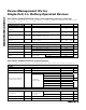
ELECTRICAL CHARACTERISTICS (OUTPUT REGULATOR) (continued)
(V
SYS_
= V
PV_
= V
IN45
= V
IN67
= 4.0V, V
BRT
= 1.25V, circuit of Figure 1, T
A
= -40°C to +85°C, unless otherwise noted.) (Note 1)
PARAMETER
SYMBOL
CONDITIONS
MIN
TYP
MAX
UNITS
LINEAR REGULATOR 5 (LDO5)
Supply Current At IN45, V
EN4
= 0V I
OUT5
= 0A
16
25 µA
Voltage Accuracy
I
OUT5
=
0 to 150mA,
V
IN45
= V
OUT5
+ 0.3V to 5.5V with 1.7V (min)
-1.5 +1.5
%
M i ni m um O utp ut C ap aci tor C
OUT5
Guaranteed stability, ESR < 0.05Ω
0.8
µF
Dropout Resistance IN45 to OUT5
0.6 1.2
Ω
Current Limit V
OUT5
= 0V
150 210
mA
LINEAR REGULATOR 6 (LDO6)
Supply Current At IN67, V
EN6
= V
SYS
, V
EN7
= 0V I
OUT6
= 0A
17
27 µA
Voltage Accuracy I
OUT6
=
0 to 300mA, V
IN67
= V
OUT6
+ 0.3V to 5.5V
-1.5 +1.5
%
M i ni m um O utp ut C ap aci tor C
OUT6
Guaranteed stability, ESR < 0.05Ω
1.76
µF
Dropout Resistance IN67 to OUT6
0.35 0.60
Ω
Current Limit V
OUT6
= 0V
300 420
mA
LINEAR REGULATOR 7 (LDO7)
Supply Current At IN67, V
EN6
= 0V, V
EN7
= V
SYS
I
OUT7
= 0A
16
25 µA
Voltage Accuracy
I
OUT7
= 0 to 150mA,
V
IN67
= V
OUT7
+ 0.3V to 5.5V with 1.7V (min)
-1.5 +1.5
%
M i ni m um O utp ut C ap aci tor C
OUT7
Guaranteed stability, ESR < 0.05Ω
0.8
µF
Dropout Resistance IN67 to OUT6
0.6 1.2
Ω
Current Limit V
OUT7
= 0V
150 210
mA
THERMAL SHUTDOWN
Thermal-Shutdown
Temperature
T
J
rising
165
°C
Thermal-Shutdown
Hysteresis
15
°C
Note 1: Limits are 100% production tested at T
A
= +25°C. Limits over the operating temperature range are guaranteed through
correlation using statistical quality control (SQC) methods.
Note 2: Input withstand voltage. Not designed to operate above V
DC
= 6.5V due to thermal-dissipation issues.
Note 3: ISET voltage when CT timer stops. Occurs only when in constant-current mode. Translates to 20% of fast-charge current.
Note 4: Temperature at which the input current limit begins to reduce.
Note 5: The WLED driver’s sink current ramp time is a function of the external compensation at CC3. With a compensation of 1kΩ in
series with 0.22µF and a target sink current of 30mA, the WLED boost’s output voltage ramps up in 1.25ms, but the WLED
sink current of 30mA settles in 12ms. See the OUT3 Enable and Disable Response graph in the
Typical Operating
Characteristics
section for more information.