
Datasheet
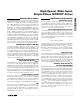

Layout Guidelines
The MAX8552 MOSFET driver sources and sinks large
currents to drive MOSFETs at high switching speeds.
The high di/dt can cause unacceptable ringing if the
trace lengths and impedances are not well controlled.
The following PC board layout guidelines are recom-
mended when designing with the MAX8552:
1) Place all decoupling capacitors as close to their
respective IC pins as possible.
2) Minimize the length of the high-current loop from
the input capacitor, the upper switching MOSFET,
and the low-side MOSFET back to the input-capaci-
tor negative terminal.
3) Provide enough copper area at and around the
switching MOSFETs and inductors to aid in thermal
dissipation.
4) Connect PGND of the MAX8552 as close as possi-
ble to the source of the low-side MOSFETs.
5) Keep LX away from sensitive analog components
and nodes. Place the IC and the analog compo-
nents on the opposite side of the board from the
power-switching node if possible.
A sample layout is available in the MAX8552 evaluation kit.
Chip Information
TRANSISTOR COUNT: 638
PROCESS: BiCMOS
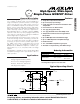
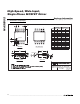
MAX8552
High-Speed, Wide-Input,
Single-Phase MOSFET Driver
_______________________________________________________________________________________ 9
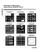
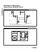
1
2
3
4
5
10
9
8
7
6
BST
DH
LX
ENGND
PGND
DL
V
CC
MAX8552
µMAX
3mm x 4.9mm
TOP VIEW
PWMDLY
1
2
3
4
5
10
9
8
7
6
BST
DH
LX
ENGND
PGND
DL
V
CC
TDFN
3mm x 3mm
PWMDLY
MAX8552
Pin Configurations