
Datasheet
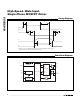

MAX8552
High-Speed, Wide-Input,
Single-Phase MOSFET Driver
2 _______________________________________________________________________________________
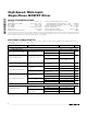
ABSOLUTE MAXIMUM RATINGS
ELECTRICAL CHARACTERISTICS
(V
CC
= V
BST
= V
DLY
= V
EN
= 5V, V
GND
= V
PGND
= V
LX
= 0V; T
A
= -40°C to +85°C, unless otherwise noted. Typical values are at T
A
=
+25°C.) (Note 1)
Stresses beyond those listed under “Absolute Maximum Ratings” may cause permanent damage to the device. These are stress ratings only, and functional
operation of the device at these or any other conditions beyond those indicated in the operational sections of the specifications is not implied. Exposure to
absolute maximum rating conditions for extended periods may affect device reliability.
V
CC
to GND..............................................................-0.3V to +7V
PWM, EN, DL, DLY to GND........................-0.3V to (V
CC
+ 0.3V)
BST to PGND..........................................................-0.3V to +35V
LX to PGND ...............................................................-1V to +28V
DH to PGND..............................................-0.3V to (V
BST
+ 0.3V)
DH, BST to LX...........................................................-0.3V to +7V
DH and DL Continuous Current......................................±200mA
Continuous Power Dissipation (T
A
= +70°C)
10-Pin µMAX (derate 5.6mW/°C above +70°C) ........444.4mW
10-Pin TDFN (derate 24.4mW/°C above +70°C) .......1951mW
Operating Temperature Range ...........................-40°C to +85°C
Junction Temperature......................................................+150°C
Storage Temperature Range .............................-65°C to +150°C
Lead Temperature (soldering, 10s) .................................+300°C
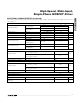
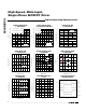
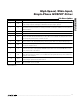
PARAMETER CONDITIONS MIN TYP MAX UNITS
UNDERVOLTAGE PROTECTION
V
CC
Supply Voltage Range 4.5 6.5 V
V
CC
rising 3.25 3.80
Undervoltage Lockout (UVLO) 0.25V hysteresis
V
CC
falling 3.0 3.5
V
PWM = GND or V
CC
,
T
A
= +25°C
0.04 1
Shutdown Supply Current V
EN
= 0V, V
CC
= 6.5V
PWM = GND or V
CC
,
T
A
= +85°C
0.1
µA
Idle Supply Current (I
CC
) No switching
V
CC
= 6.5V, PWM = GND,
R
DLY
= 47kΩ
330 500 µA
PWM = GND 25 50 µA
No switching
PWM = V
CC
23mA
Control Supply Current (I
GND
)
Switching
f
PWM
= 250kHz,
50% duty cycle
1.8 3 mA
PWM = GND 0.1 10 µA
No switching, I
CC
PWM = V
CC
1.2 2 mA
PWM = GND 0.1 10 µA
No switching, I
BST
PWM = V
CC
1.2 2
Driver Supply Current (I
PGND
)
Switching, I
BST
+ I
CC
250kHz 2 4
mA
DRIVER SPECIFICATIONS (See the Timing Diagram)
V
BST
= 4.5V 1.3 2.4
PWM = GND,
sourcing current
V
BST
= 5V 1.2
V
BST
= 4.5V 0.7 1.1
DH Driver Resistance
PWM = V
CC
,
sinking current
V
BST
= 5V 0.6
Ω