
Datasheet


MAX8505
3A, 1MHz, 1% Accurate, Internal Switch
Step-Down Regulator with Power-OK
_______________________________________________________________________________________ 5
Note 1: Under normal operating conditions, COMP moves between 1.25V and 2.15V as the duty cycle changes from 10% to 90%
and peak inductor current changes from 0 to 3A. Maximum output current is related to peak inductor current, inductor value
input voltage, and output voltage by the following equations:
where V
OUT
= output voltage; I
LIM
= current limit of high-side switch; t
S
= switching period; R
L
= ESR of inductor; R
NLS
=
on-resistance of low-side switch; L = inductor. Equations for I
LIM
and D are shown as follows:
where I
LIM_DC100
= current limit at D = 100%; R
T
= transresistance from LX to COMP; V
SW
= slope compensation (310mV
±20%); D = duty cycle:
where V
OUT
= output voltage; V
IN
= input voltage; I
O
= output current; R
L
= ESR of inductor; R
NHS
= on-resistance of high-
side switch; R
NLS
= on-resistance of low-side switch. See the
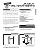
Typical Application Circuit
for external components.
Note 2: Specifications to -40°C are guaranteed by design and not production tested.
Note 3: LX has internal clamp diodes to PGND and IN pins 2 and 4. Applications that forward bias these diodes should take care
not to exceed the IC’s package power dissipation limits.
Note 4: When connected together, the LX output is designed to provide 3.5A
RMS
current.
D
VIRR
VIR R
OUT O NLS L
IN O NLS NHS
=
++
+−
()
()
II V
D
R
LIM LIM DC SW
T
=+
−
_ 100
1
I
IDtVL
Dt R R L
OUT MAX
LIM S OUT
S NLS L
_
() /
() ( )/
=
−− × ×
+− × × +
12
11 2
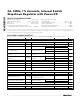
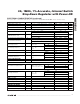
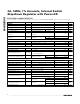
ELECTRICAL CHARACTERISTICS (continued)
(V
IN
= V
CC
= V
CTL
= +3.3V, V
FB
= 0.8V, V
COMP
= 1.25V, C
REF
= 0.01µF, T
A
= -40°C to +85°C, unless otherwise noted.) (Note 2)
PARAMETER SYMBOL CONDITIONS MIN TYP MAX UNITS
500kHz 90
LX Maximum Duty Cycle
V
IN
= V
CC
= 2.6V, 3.3V,
5.5V
1MHz 84
%
500kHz 8
LX Minimum Duty Cycle
V
IN
= V
CC
= 2.6V, 3.3V,
5.5V
1MHz 15
%
SLOPE COMPENSATION
Slope Compensation Extrapolated to 100% duty cycle 245 406 mV
BST
V
LX
= 5.5V
10
V
LX
= 0V 10
BST Shutdown Supply Current
(V
BST
- V
LX
) = V
IN
=
V
CC
= 5.5V, V
CTL
= 0V
LX open 10
µA
CTL
For 1MHz 80
For 500kHz 55 70
CTL Input Threshold
V
IN
= V
CC
= 2.6V,
3.3V, 5.5V
For shutdown 45
% of
V
CC
CTL Input Current V
CTL
= 0V or 5.5V, V
IN
= V
CC
= 5.5V -1 +1 µA
POK (Power-OK)
POK Output Voltage, Low V
FB
= 0.6V or 1.0V, I
POK
= 2mA 100 mV
POK Leakage Current V
POK
= 5.5V 1 µA
POK Fault Delay Time From FB to POK, any threshold 25 100 µs