
Datasheet
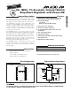


MAX8505
3A, 1MHz, 1% Accurate, Internal Switch
Step-Down Regulator with Power-OK
2 _______________________________________________________________________________________
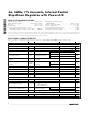
ABSOLUTE MAXIMUM RATINGS
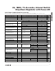
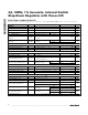
ELECTRICAL CHARACTERISTICS
(V
IN
= V
CC
= V
CTL
= +3.3V, V
FB
= 0.8V, V
COMP
= 1.25V, C
REF
= 0.01µF, T
A
= 0°C to +85°C, unless otherwise noted.)
Stresses beyond those listed under “Absolute Maximum Ratings” may cause permanent damage to the device. These are stress ratings only, and functional
operation of the device at these or any other conditions beyond those indicated in the operational sections of the specifications is not implied. Exposure to
absolute maximum rating conditions for extended periods may affect device reliability.
CTL, FB, IN, V
CC
to GND .........................................-0.3V to +6V
COMP, REF, POK to GND..........................-0.3V to (V
CC
+ 0.3V)
BST to LX..................................................................-0.3V to +6V
PGND to GND .......................................................-0.3V to +0.3V
Continuous Power Dissipation (T
A
= +70°C)
16-Pin QSOP (derate 12.5mW/°C above +70°C).......1000mW
Operating Temperature Range
MAX8505EEE...................................................-40°C to +85°C
Storage Temperature Range .............................-65°C to +150°C
Junction Temperature......................................................+150°C
Lead Temperature (soldering, 10s) .................................+300°C
Soldering Temperature (reflow) .......................................+260°C
PARAMETER SYMBOL CONDITIONS MIN TYP MAX UNITS
IN AND V
CC
IN Voltage Range V
IN
2.25 V
CC
V
V
CC
Voltage Range V
CC
2.6 5.5 V
V
IN
= 3.3V 6
10
IN Supply Current I
IN
Switching with no load
V
IN
= 5.5V 10
mA
V
CC
= 3.3V 3
10
V
CC
Supply Current I
CC
Switching with no load
V
CC
= 5.5V 6
mA
Total Shutdown Current into IN
and V
CC
I
SHDN
V
IN
= V
CC
= V
BST
- V
LX
= 5.5V, V
CTL
= 0V,
V
LX
= 0V
20 50 µA
V
CC
rising 2.40 2.55
V
CC
Undervoltage Lockout
Threshold
UVLO
th
When LX starts/stops
switching
V
CC
falling 2.2 2.35
V
REF
REF Voltage V
REF
I
REF
= 0µA, V
IN
= V
CC
= 2.6V to 5.5V 0.792 0.800 0.808 V
REF Shutdown Resistance From REF to GND, V
CTL
= 0V 13 100 Ω
REF Soft-Start Current V
REF
= 0.4V 20 25 30 µA
Soft-Start Ramp Time
Output from 0% to 100%, C
REF
= 0.01µF to
1µF
32 ms/µF
FB
FB Regulation Voltage V
IN
= 2.6V to 5.5V 0.792 0.800 0.808 V
FB Input Bias Current V
FB
= 0.7V 0.01 0.1 µA
Maximum Output Current I
OUT_MAX
V
IN
= V
CC
= 3.3V, V
OUT
= 1.2V,
L = 1µH/5.9mΩ (Note 1)
3A
FB high
10.5 12 13.5
FB Threshold for POK Transition FB rising or falling
FB low -13.5 -12 -10.5
%
FB to POK Delay FB rising or falling 50 µs
COMP
COMP Transconductance From FB to COMP 60 100 160 µS
Gain from FB to COMP V
COMP
= 1.25V to 1.75V 80 dB